Parity generator
Task: Design a circuit that generates the parity bit of an 8-bit word. The 8-bit word should be given through manual switches SW0-SW7 on the prototype board (in remote mode – through virtual switches SW0-SW7 connected to the prototype board ). Parity bit should be displayed on the LED display by means of the following symbols: E – means even number of ‘ones’ in the 8-bit input word, O – means odd number of ‘ones’.
Perform a functional simulation and verify the system practically by programming a prototype FPGA board.
On the prototype board, there are 8 seven-segment displays with a common anode, connected in a multiplexed manner. The right half (4 digits) of the 7-segment display is in use (the left half may also display something - ignore it). The result should be displayed on the AN0 display. Multiplexed connection is made by common connection of all segment outputs, i.e. connection of A segments in all displays, connection of B segments in all displays, etc. Common anodes are used to activate a given display. The individual segments of a single display are activated by giving a low state to A - G pins. Switching on individual displays is activated by a low state on AN0 - AN3 pins (inverted common anode). For example, if we want to disable displays 1-3, then logic '1' should be set on AN1 - AN3 pins. If at the same time we want to display the sign "A" on the display 0, then additionally the following signals should be given: AN0 = '0' and A='0', B='0', C='0', D='1', E='0', F='0', G='0', DP='1'.
Minimum requirements for simulation and verification on the board: initialize all the switches to OFF, then (in the simulation every 100 ms) set the consecutive switches to ON until all switches are ON.
Part of the main (top level) VHDL design file with signal declaration:
entity top is
Port ( sw_i : in STD_LOGIC_VECTOR (7 downto 0);
led7_an_o : out STD_LOGIC_VECTOR (3 downto 0);
led7_seg_o : out STD_LOGIC_VECTOR (7 downto 0));
end top;
In led7_seg_o, segment A is connected to bit 7, segment B to bit 6, etc.
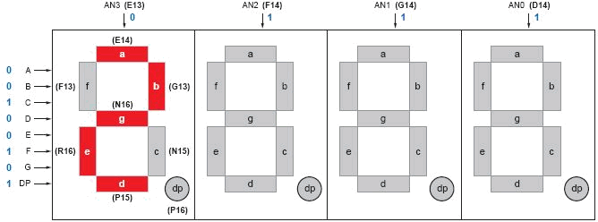
Fig.
1. Description of connections of individual display segments. Example of
displaying the digit '2'.
Design constraints file for Nexys-A7 board (FPGA chip xc7a100tcsg324-1): iup1s.xdc
Design constraints file for remote mode (with support for virtual switches): iup1z.xdc
The following Vivado warnings can be ignored for this exercise:
[Power 33-232] No user defined clocks were found in the design! Power estimation will be inaccurate until this is corrected.
[Timing 38-313] There are no user specified timing constraints. Timing constraints are needed for proper timing analysis.
[Place 46-29] place_design is not in timing mode. Skip physical synthesis in placer.