Task: The main goal of the exercise is to develop a module that controls the four digits of the LED display for use in the following exercises.
To check the operation of this block, it must be embedded in a system that allows setting (using buttons and switches) and displaying any 4-digit hexadecimal number (with DP) on the LED display. Then a functional simulation should be performed and the system should be verified by programming the FPGA board.
The right half (4 digits) of the 8-digit 7-segment display present on the prototype board is in use (the left half may also display something - we ignore it).
The display controller block should have the following interface (this block will be used in the following exercises):
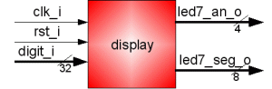
Fig. 1 Interface of the display control block.
Inputs:
- clk_i – 100 MHz clock,
- rst_i – asynchronous reset active with high state '1'. During the activity of the rst_i signal, all display segments should light up,
- digit_i – 32-bit input, each bit corresponds to a specific segment (the oldest 8 bits refer to the digit AN3, etc.).
Outputs:
- led7_an_o – output controlling display anodes (determines which display is on),
- led7_seg_o – output controlling display segments (determines which segments are turned on).
The display consists of four 7-segment LED displays. The respective segments of
the individual displays are connected, so multiplexing has to be applied. To
light the appropriate segment, output a logic '0' both to the digit (ANx) and
to the segment (A-G or DP). The required multiplexing frequency is 1 kHz (i.e.
every 1 ms the display switches to the next digit). The system clock frequency
(100 MHz) divisor resulting in the multiplexing frequency (1 kHz) should be a
changeable parameter of the display component.
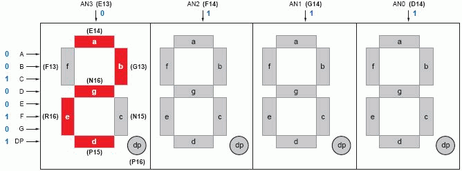
Fig.
2 Description of connections of individual display signals. An example of
displaying the digit '2'.
Then you need to implement the second component - the encoder and display memory. It is used to test the display block and should allow the following operations:
1) Set the 4-bit value using the switches: SW3, SW2, SW1, SW0.
2) Pressing the BTNL button (BTN3 in the remote mode) will light the AN3 digit of the display with the currently set value on the SW3-SW0 switches. The value should be displayed in a hexadecimal form. The same action should be assigned to the other buttons, i.e. respectively: pressing BTNC (BTN2 in the remote mode) causes AN2, BTNR (BTN1) → AN1 and BTND (BTN0) → AN0 digits to light up. After pressing and releasing the button, the sign on the display should remain lit until a new value is entered.
3) Turning on the SW7 switch should cause the lighting of the DP (decimal point) of the AN3 display. Turning off the switch should cause the DP of this display to go out. The same operation also applies to SW6 → DP AN2, SW5 → DP AN1, SW4 → DP AN0. The operation of this function shall be independent of the state of the BTNx buttons.
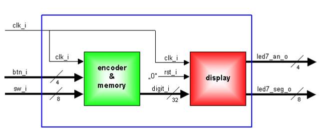
Fig. 3 Block diagram
of the test system.
Minimum simulation requirements: simulate pressing and releasing consecutive BTNx buttons. The time of pressing the button should be 1 ms, and the release time 2 ms. In the middle of the time interval between releasing and pressing the button, change the state of switches SW3-0 to different hexadecimal value. At the beginning, set the state of SW7-4 switches so that 2 arbitrarily selected dots light up. The state of these switches should be changed at least 2 times to another (during the change, the BTNx buttons should be released). The simulation should be allowed to run until the process of displaying all the entered digits and the change of the dot state is visible.
An example of this simulation was also presented as waveforms at the end of the presentation: Demonstracja VIVADO (in Polish)
Minimum requirements for verification on the board: enter the number of the student's index (in the case of a group – the index number of any student from the group) on the LED display in hexadecimal form, where the most significant digits are to be entered on the 7-segment displays, and the least significant digit is presented by means of dots (the MSB bit on the left side, the dot is on - means 1).
Part of the main (top level) VHDL design file with signal declaration:
entity top is
Port ( clk_i : in STD_LOGIC;
btn_i : in STD_LOGIC_VECTOR (3 downto 0);
sw_i : in STD_LOGIC_VECTOR (7 downto 0);
led7_an_o : out STD_LOGIC_VECTOR (3 downto 0);
led7_seg_o : out STD_LOGIC_VECTOR (7 downto 0));
end top;
Remark:
btn_i(3) – button BTNL (BTN3)
btn_i(2) – button BTNC (BTN2)
btn_i(1) – button BTNR (BTN1)
btn_i(0) – button BTND (BTN0)
Design constraints file for Nexys-A7 board (FPGA chip xc7a100tcsg324-1): iup6s.xdc
Design constraints file for remote mode (with support for virtual buttons and switches): iup6z.xdc