Core
Generator (version 1)
Exercise: Redesign
previous RS232 project in the following way:
The system should buffer data received from RS232 port. After the
„row_max” number of characters is collected the system should print them back
to RS-232 port in the pseudo-graphic form (using printed character as a pixel).
Besides, the system should buffer input characters coming from RS232
port in the printout phase. The length
of the buffer should be 64 characters. Buffer overflow should be signaled by
LD0 LED (LED should be on during overflow condition). RS232 port parameters
should be identical to those used in last exercise, also RS232 port monitoring
function (on LED display) should be left intact. row_max parameter should be easily modifiable (for example defined
as a constant) and should accept values from 2 to 15.
Below sample printout of several lines is presented (row_max=8):
bbb ddd
fff hhh
bb dd
ff ff hh
bb
dd ff f
hh
aaaa
bbbbb cccc dddd
eeee ff ggg gg hh
aa
bb bb cc cc dd dd
ee ee fffff gg gg
hhhhh
aaaaa
bb bb cc dd dd
eeeeee ff gg
gg hh hh
aa aa
bb bb cc dd dd
ee ff gg
gg hh hh
aa aa
bbb bb cc cc
dd dd ee ee ff
ggggg hh hh
aaa aa bbb bb cccc ddd dd eeee
ffff gg hhh hh
gg gg
gggg
AA
BBBBBB CCC DDDDD
EEEEEE FFFFFF GGGG
HH HH
AAAA
BB BB CC CC DD DD EE
E FF F GGG GG HH
HH
AA
AA BB BB CC C
DD DD EE FF GG
HH HH
AA
AA BB BB CC DD
DD EE E FF F
GG HH HH
AA
AA BBBBB CC
DD DD EEEE FFFF GG
HHHHHH
AAAAAA
BB BB CC DD DD
EE E FF F GG GGG
HH HH
AA
AA BB BB CC C
DD DD EE FF GG
GG HH HH
AA
AA BB BB CC CC DD DD
EE E FF GGG GG HH
HH
AA AA
BBBBBB CCC DDDDD EEEEEE FFFF
GGGG HH HH
11
2222 3333 44
555555 666 777777
8888
111
22 22 33 33 444
55 66 77
77 88 88
1111
22 33 4444
55 66 77
88 88
11
22 33 44 44
55 66 77
88 88
11
22 3333 44
44 55555 66666
77 8888
11
22 33 4444444 55
66 66 77 88 88
11
22 33 44 55 66
66 77 88
88
11
22 22 33 33 44
55 55 66 66 77
88 88
1111
222222 3333 4444
5555 6666 77
8888
Characters which codes are below 32 should be printed using asterisks
(*) as pixels. Do not implement control functions of those characters (like
Line Feed, Carriage Return, etc.). Example of line containing characters which
codes are below 32 is presented below:
****
**** ***** *****
***** ***
*
* ** ** *** * * ******* ** ** * *****
****
** ** ** * * * * * ** * ** *******
*** *****
*
** ** ** * * * ******* ******* *****
***
*
**** **** *
* ******* ******* ******* *******
*
** ** ** *
*** * ** ** ******* *****
*******
**
****** ** **
* * * *** *** ***** ***
*****
*** **
** ** * * ******* ***
* *
** **
**** ***** *****
* *****
Inputs and outputs of the circuit:
clk_i - clock 50MHz,
rst_i – asynchronous reset,
RXD_i – data input RS232,
TXD_o – data output RS232,
ld0 – output of FIFO buffer overflow signal (LED LD0),
led7_an_o – output to LED-display anodes,
led7_seg_o
–
output to LED-display segments.
For project implementation you will need two functional modules
generated by Core Generator application.
ROM (Read Only Memory) will provide characters fonts. FIFO memory will
be used as 64-character input buffer. Character definitions (8x16) can be downloaded
here: chargen.coe
ROM module generation:
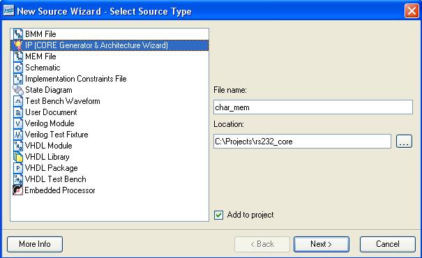
Choose:
Project -> New Source
This
will open a new window Select Source Type in which choose:
IP (CORE Generator & Architecture Wizard).
Enter the file name for new component (generated by Core Generator), for
example: char_mem and click Next:
The
window ”Select IP” for new component choice will be opened:
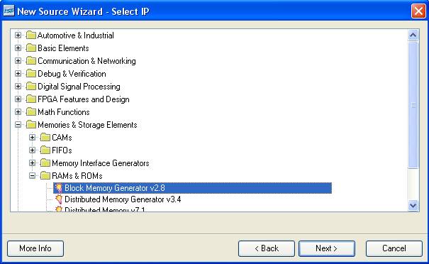
In this
window we choose Block Memory Generator v2.8 and we click Next.
Next the summary window will show up: New Source Wizard – Summary. It
must be acknowledged by clicking Finish.
Next
the Core Generator starts and the new window for component configuration is
opened:
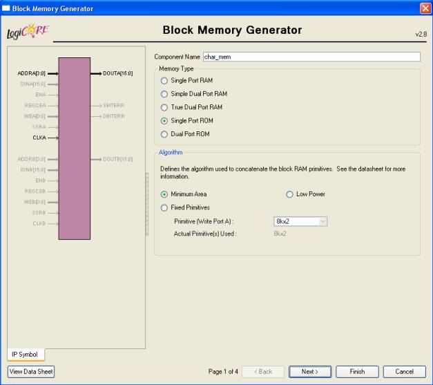
In this
window (1/4) change Memory Type to Single Port ROM.
You can use View Data Sheet button (in down-left corner) to open
detailed documentation of configured component.
Then
click Next.
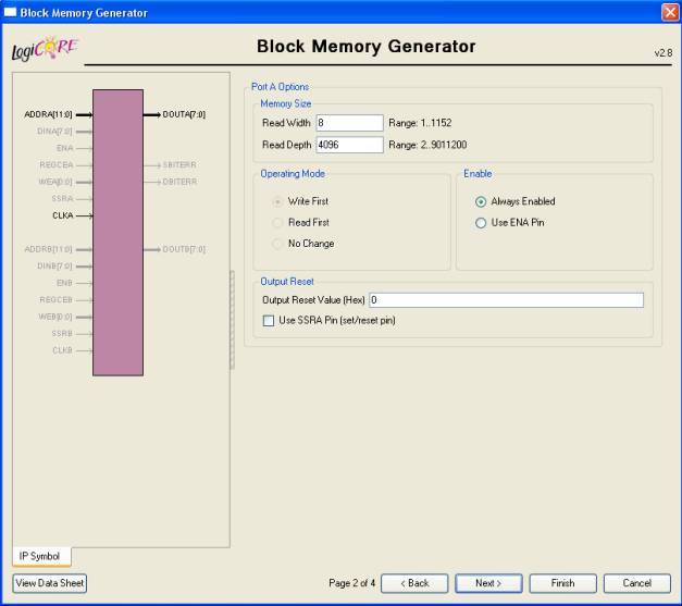
In this
window (2/4) change Read Width to 8 (characters are defined with
8 pixels in horizonal direction) and Read
Depth to 4096 (there are 256
characters defined, and each occupy 16 bytes in the memory).
Then
click Next.
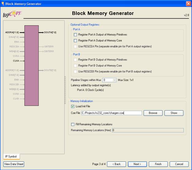
In this
window (3/4) mark Load Init File and enter path to the file chargen.coe with characters definitions (you can make
this easy by using Browse button).
Then
click Next.
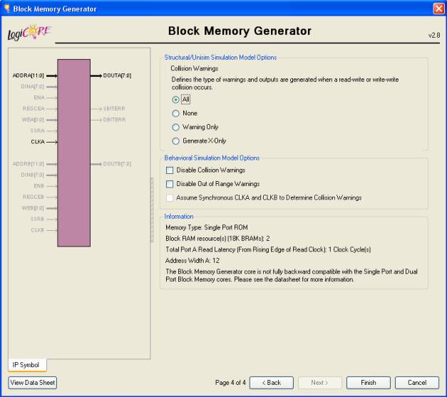
In this
window (4/4) change nothing. But, it is worth to remember helpful project
summary information (Information field) and the block symbol of designed
component. The most important information is: Total Port A Read Latency
(From Rising Edge of Read Clock): 1 Clock Cycle(s)
Acknowledge
by pressing Finish.
The
component generation will begin – please wait a moment.
After
the successful generation component will be added to the list of project files.
Below the
definition of characters in the generated ROM is presented: (using letter R as
an example):
|
Address |
b7 |
b6 |
b5 |
b4 |
b3 |
b2 |
b1 |
b0 |
|
ascii*16+0 |
0 |
0 |
0 |
0 |
0 |
0 |
0 |
0 |
|
ascii*16+1 |
0 |
0 |
0 |
0 |
0 |
0 |
0 |
0 |
|
ascii*16+2 |
0 |
1 |
1 |
1 |
1 |
0 |
0 |
0 |
|
ascii*16+3 |
0 |
1 |
0 |
0 |
0 |
1 |
0 |
0 |
|
ascii*16+4 |
0 |
1 |
0 |
0 |
0 |
1 |
0 |
0 |
|
ascii*16+5 |
0 |
1 |
0 |
0 |
0 |
1 |
0 |
0 |
|
ascii*16+6 |
0 |
1 |
0 |
0 |
0 |
1 |
0 |
0 |
|
ascii*16+7 |
0 |
1 |
1 |
1 |
1 |
0 |
0 |
0 |
|
ascii*16+8 |
0 |
1 |
0 |
1 |
0 |
0 |
0 |
0 |
|
ascii*16+9 |
0 |
1 |
0 |
0 |
1 |
0 |
0 |
0 |
|
ascii*16+10 |
0 |
1 |
0 |
0 |
1 |
0 |
0 |
0 |
|
ascii*16+11 |
0 |
1 |
0 |
0 |
0 |
1 |
0 |
0 |
|
ascii*16+12 |
0 |
1 |
0 |
0 |
0 |
1 |
0 |
0 |
|
ascii*16+13 |
0 |
0 |
0 |
0 |
0 |
0 |
0 |
0 |
|
ascii*16+14 |
0 |
0 |
0 |
0 |
0 |
0 |
0 |
0 |
|
ascii*16+15 |
0 |
0 |
0 |
0 |
0 |
0 |
0 |
0 |
Address –
address in the ROM.
ascii –
ASCII code of printed character.
Address
for the ROM can be easily generated by concatenating 8-bit vector of ASCII code
with 4-bit vector of line number of character (0-15) using the & operator.
Remember that after printing the line you should send two control characters:
CR (code: 13) and LF (code: 10) to make the cursor go to the new line.
For
easy component instantiation files with *.vho extension are created. They
contain the template of component declaration and example of how to make the
instance of the component. You can easily include those files in the project
files.
Sample
VHO file:
-- The following code must
appear in the VHDL architecture header:
------------- Begin Cut here for COMPONENT Declaration ------ COMP_TAG
component char_mem
port (
clka: IN std_logic;
addra: IN std_logic_VECTOR(11
downto 0);
douta: OUT std_logic_VECTOR(7
downto 0));
end component;
-- Synplicity black box declaration
attribute syn_black_box : boolean;
attribute syn_black_box of char_mem: component is true;
-- COMP_TAG_END ------ End COMPONENT Declaration ------------
-- The following code must appear in the VHDL architecture
-- body. Substitute your own instance name and net names.
------------- Begin Cut here for INSTANTIATION Template ----- INST_TAG
your_instance_name : char_mem
port map (
clka => clka,
addra => addra,
douta => douta);
-- INST_TAG_END ------ End INSTANTIATION Template ------------
-- You must compile the wrapper file char_mem.vhd when simulating
-- the core, char_mem. When compiling the wrapper file, be sure to
-- reference the XilinxCoreLib VHDL simulation library. For detailed
-- instructions, please refer to the "CORE Generator Help".
Text
with red font should be copied to the local
signal definition area. Text with blue font
should be copied to the architecture area (of course connected signals and
instance name should be changed as needed). Then the icon representing new
component should be automatically moved to the proper place in the project’s
hierarchy.
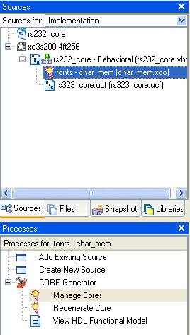
Modification
of component parameters and its regeneration is possible using icons: Manage
Cores i Regenerate Core
presented below:
Generation of FIFO memory module:
To
generate the FIFO module proceed as before:
Choose: Project -> New Source
In the
window Select Source Type choose: IP (CORE Generator & Architecture
Wizard).
Enter the file name for new component, for example: fifo_mem and click Next:
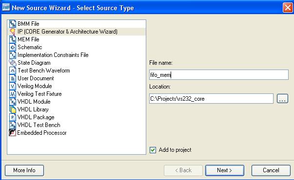
Next
window will be opened - Select IP:
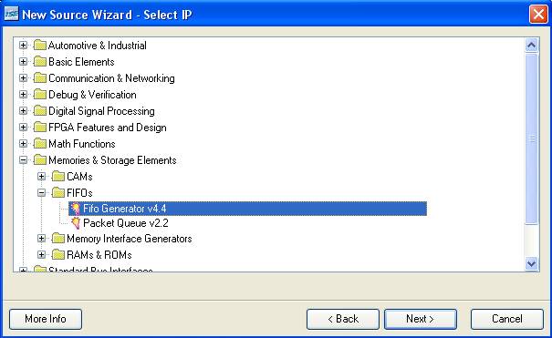
In this
window choose Fifo Generator v4.4 and click
Next.
Next the summary window appears: New Source Wizard – Summary.
You should acknowledge by pressing Finish.
Then
the Core Generator starts and the component configuration widow is opened:
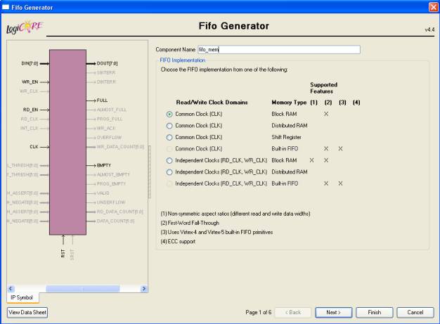
In this
window (1/6) choose option: Common Clock (CLK) – Block RAM.
Use View Data Sheet button to see complete and detailed documentation of
the core.
Then
click Next.
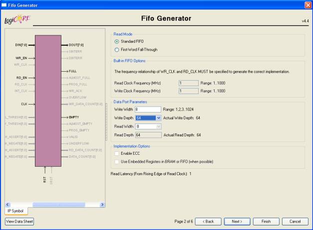
In this
window (2/6) change Write Width to 8, Write Depth to 64
(assumed FIFO capacity) and Read
Width to 8.
Please notice the information on the bottom of the page (it is generated based
on previously set options and is important for FIFO reads):
Read Latency (From Rising Edge of Read Clock): 1
Then
click Next four times (leave the options of the next 4 windows
unchanged). Last window (6/6) should be printed like below:
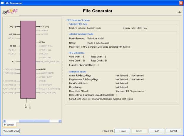
It is
worth to remember helpful information containing summary of the properties of
designed component (field Information).
Confirm
it by pressing Finish.
The
component generation procedure starts – please wait a moment.
Now you
have to instantiate the component in your project using *.vho file (procedure
is similar to described previously in ROM component).
Important
information about the FIFO component can also be found in UG175
document.
The circuit has to verified experimentally by
programming the FPGA on development board. You can also perform functional
simulation if you need. After the FPGA is programmed check the basic
functionality of the system: print some lines on terminal and check the buffer
overflow detection (by keeping any key pressed for about 30
seconds). For testing use MINICOM
terminal emulation program (MINICOM is by default configured as follows:
9600bps, 8 data bits, 1 stop bit, no parity). Show the results to the
instructor.
Transmission and reception of data
in RS232 standard:
Transmission
and reception of RS232 signals is serial.
When the line is idle logic level on the input and output line is “1”.
Beginning of the transmission is signaled by the falling edge of the input
signal followed by “0” level lasting for 1/baud_rate seconds (where baud_rate
is the speed parameter of RS232). In the example start bit (and all other bits)
lasts for 1/9600 second each. Data bits follow start bit and are send serially
LSB first. Then the optional parity bit can be sent (but it is not present in
our example – parity is disabled in the RS232 settings). The end of
transmission is signaled by the stop bit which has logic level “1”. Example of transmission of the code: 01010011 is presented below:
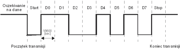
Fig.1 Transmission of the code: 01010011 using RS-232
(9600 bps, 8-bits, 1-stop, no parity).
Additional information about RS232:
http://www.fizyka.umk.pl/~ptarg/labview/folie/RS232.pdf
http://pl.wikipedia.org/wiki/RS-232
UCF file for the exercise (for
Digilent Spartan-3 board, FPGA: Spartan-3 3S200 FT256-4):
# Clock:
NET "clk_i" LOC = "T9" ; # 50 MHz clock
# Push-buttons:
NET "rst_i" LOC = "L14" ; # pressed high BTN3
# RS232:
NET "TXD_o" LOC = "R13" ; # RS 232 TXD
NET "RXD_i" LOC = "T13" ; # RS 232 RXD
# Seven-segment LED display:
NET "led7_an_o<3>" LOC = "E13" ; # leftmost digit,
active low
NET "led7_an_o<2>" LOC = "F14" ; # active low
NET "led7_an_o<1>" LOC = "G14" ; # active low
NET "led7_an_o<0>" LOC = "D14" ; # rightmost digit,
active low
NET "led7_seg_o<7>" LOC = "E14" ; # segment 'a',
active low
NET "led7_seg_o<6>" LOC = "G13" ; # segment 'b',
active low
NET "led7_seg_o<5>" LOC = "N15" ; # segment 'c',
active low
NET "led7_seg_o<4>" LOC = "P15" ; # segment 'd',
active low
NET "led7_seg_o<3>" LOC = "R16" ; # segment 'e',
active low
NET "led7_seg_o<2>" LOC = "F13" ; # segment 'f',
active low
NET "led7_seg_o<1>" LOC = "N16" ; # segment 'g',
active low
NET "led7_seg_o<0>" LOC = "P16" ; # segment 'dp',
active low
# LD0 LED:
NET "ld0" LOC = "K12" ; # high on
#