Core
Generator (version 2)
Task: Implement the Lissajous curve
generator with the following properties:
- The curve
should be presented in a square field of 384x384 pixels.
- The picture
should be generated on an analog VGA monitor (you can use 640x480 mode).
- The picture
should be centered and square shaped on the display.
- The curve
should be white, the background should be black.
- The
frequencies of the channels (X and Y) and the phase of the second channel
(Y) should be configurable using the switches: SW0-SW7 (range 0-255) which
define the value to be loaded to the registers by pressing the buttons:
BTN0 (loads the X frequency register), BTN1 (loads the Y frequency
register), BTN2 (loads the Y phase offset register).
- The BTN3
button should clear the screen and reset the DDS generator (to make the
figure being redrawn starting from the programmed initial phase for the
channel Y and the zero phase for the channel X).
- The channel X
should be the channel 0 in the DDS component description.
- The channel Y
should be the channel 1 in the DDS component description.
- The
coordinates (0,0) should be in the center of the screen. The curve should
use the entire 384x384 field.
Information about the
Lissajous curve
Ports’ usage:
- clk_i – 50MHz clock
input,
- rgb_o – RGB output
(to an analog VGA display),
- hsync_o – horizontal
sync output (to an analog VGA display),
- vsync_o – vertical
sync output (to an analog VGA display),
- sw_i – switches
for setting the frequencies and phases of the channels,
- btn_i –
pushbuttons for loading the frequencies and phases to the DDS.
Information
about the analog VGA signal generation
Remember that the RGB output should be at the logic level ‘0’ when the
current sync phase is out of the display area.
For project implementation two functional modules generated by the Core
Generator will be needed. Dual
port RAM memory will be used as a display memory. Direct Digital Synthesizer will be used for digital
sinusoidal signal generation (two channels: X and Y).
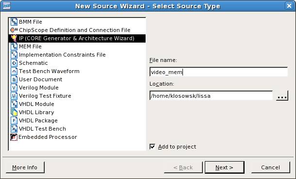
Video memory generation:
Choose:
Project -> New Source
In the
window: Select Source Type select:
IP (CORE Generator & Architecture Wizard).
Enter the file name of a new component (to be generated by the Core Generator),
for example: video_mem and click Next:
Next
window (Select IP) is for a new component selection:
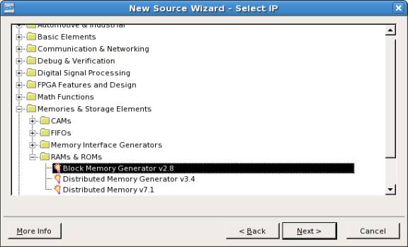
In this
window choose Block Memory Generator v2.8 and click Next. Then
the summary window appears: New Source Wizard – Summary. Acknowledge by
clicking Finish.
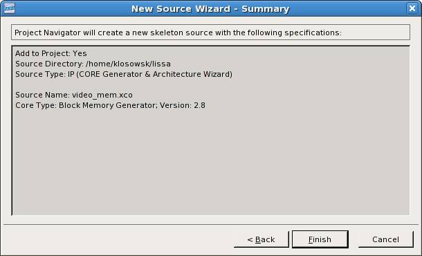
The
Core Generator starts and a new window for detailed component configuration is
opened:
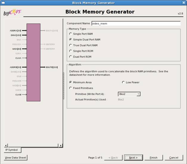
In the
first window (1/5) change Memory Type to Simple Dual Port RAM.
The dual port memory will be used for simultaneous writing and reading from two
different addresses (pixels of the curve are written, sequential pixels for the
VGA display are read).
View Data Sheet button (in left-down corner) opens a detailed
documentation of the component.
Click: Next.
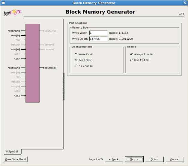
In this
window (2/5) change Write Width to 1 (we will write only one
pixel at the location calculated by the curve generator) and Write Depth to
147456 (there are 384*384 = 147456 pixels).
Click Next.
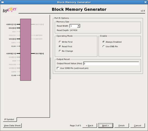
In this
window (3/5) change Read Width to 1 (we will read only one pixel
at the location calculated by the VGA display generator). It is possible to set
different size of the input and output data bus for this memory component if
you need. Address count is now calculated automatically.
Click Next.
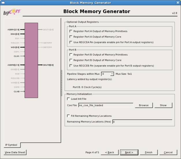
In this
window (4/5) nothing should be changed. The initial memory contents – all bits
zeroed.
Click Next.
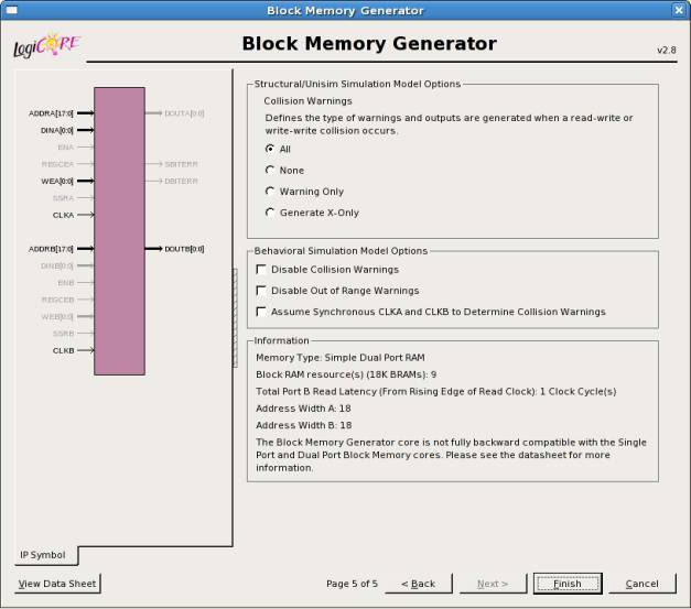
In this
window (5/5) nothing should be changed. This window can be used to set
parameters of the simulation model for the memory (collision detection and
range warnings).
Click Finish.
Now the
component generation starts – please wait a moment.
The
generated memory has two clock inputs (one for each port) - it can be used if
we have two clock domains. But usually we only have one clock in the design and
in this situation we connect two clock inputs to the same clock.
Pay
attention to signal types of generated component, some of them are 1-bit
vectors (like WEA).
It is
worth to remember additional information presented in the summary of a
properties of designed component (Information field) and the schematic
diagram. Important information for designer is:
Total Port B Read Latency (From Rising Edge of Read Clock): 1 Clock
Cycle(s).
It
means that data is read from the memory with a delay of one clock cycle after
the address is latched. Write procedure is different: written data should be
latched at the same time as address. For details see the documentation (use View
Data Sheet button).
After
generation the new component will be added to the list of project’s files.
For
easy component instantiation files with *.vho extension are created. They
contain the template of component declaration and example of how to make the
instance of the component. You can easily include those files in the project
files.
Sample
VHO file:
--------------------------------------------------------------------------------
-- The
following code must appear in the VHDL architecture header:
-------------
Begin Cut here for COMPONENT Declaration ------ COMP_TAG
component
video_mem
port (
clka: IN std_logic;
dina: IN std_logic_VECTOR(0 downto 0);
addra: IN std_logic_VECTOR(17 downto 0);
wea: IN std_logic_VECTOR(0 downto 0);
clkb: IN std_logic;
addrb: IN std_logic_VECTOR(17 downto 0);
doutb: OUT std_logic_VECTOR(0 downto 0));
end
component;
--
Synplicity black box declaration
attribute
syn_black_box : boolean;
attribute
syn_black_box of video_mem: component is true;
--
COMP_TAG_END ------ End COMPONENT Declaration ------------
-- The
following code must appear in the VHDL architecture
-- body.
Substitute your own instance name and net names.
-------------
Begin Cut here for INSTANTIATION Template ----- INST_TAG
your_instance_name
: video_mem
port map (
clka => clka,
dina => dina,
addra => addra,
wea => wea,
clkb => clkb,
addrb => addrb,
doutb => doutb);
--
INST_TAG_END ------ End INSTANTIATION Template ------------
-- You must
compile the wrapper file video_mem.vhd when simulating
-- the
core, video_mem. When compiling the wrapper file, be sure to
--
reference the XilinxCoreLib VHDL simulation library. For detailed
--
instructions, please refer to the "CORE Generator Help".
The
text in red font should be copied to the local
signal definition area. The text in blue font
should be copied to the architecture area (of course the connected signals’
names and the instance name should be changed as needed). Then the icon
representing the new component should be automatically moved to the proper
place in the project’s hierarchy.
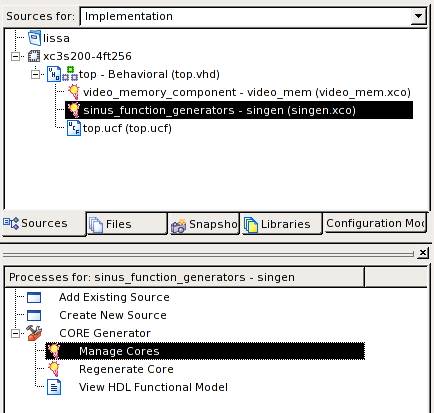
Modification
of component parameters and its regeneration is possible using icons: Manage
Cores i Regenerate Core
presented below:
DDS module generation
To
generate the DDS module proceed as follows:
Choose:
Project -> New Source
In the
window Select Source Type choose: IP (CORE Generator & Architecture
Wizard).
Enter the file name of a new component, for example: singen and click Next:

Next
window will be opened - Select IP:
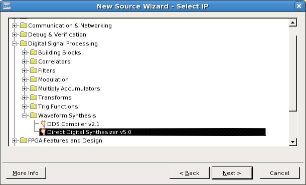
In this
window choose Direct Digital
Synthesizer v5.0 and click Next.
Next the summary window appears: New Source Wizard – Summary.
You should acknowledge by pressing Finish.

Then
the Core Generator starts and the component configuration widow is opened:
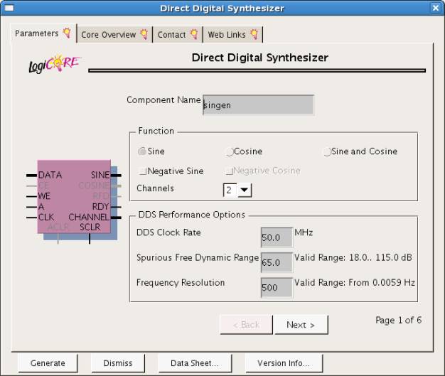
In this
window (1/6) choose function: Sine
and the number of channels: Channels: 2.
(you will need two independent sine function generators to draw the Lissajous
curves). Then enter the system clock frequency – DDS Clock Rate: 50 MHz.
You have to decide about the quality of the generated signal, choose - Spurious Free Dynamic Range: 65 dB (SFDR is the ratio of the RMS amplitude
of the generated frequency to the RMS amplitude of the largest noise or
harmonic distortion component).
In the end specify the frequency resolution for the sine signal: Frequency Resolution: 500 Hz
Use View Data Sheet button to see the complete and detailed
documentation of the core.
Then
click Next.
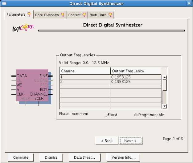
In this
window (2/6) set initial channel frequencies (enter frequency in MHz). Set the
frequency to: 0.1953125 MHz for
each channel.
Warning – due to a software bug it is difficult to see typed numbers. When
finally entered the value is displayed correctly.
Phase Increment set to:
Programmable – you will be therefore allowed to change the frequency later
in the system. The frequency will be set using the slide switches – load the
value to the eight least significant bits of the configuration word.
Then
click Next.
In this
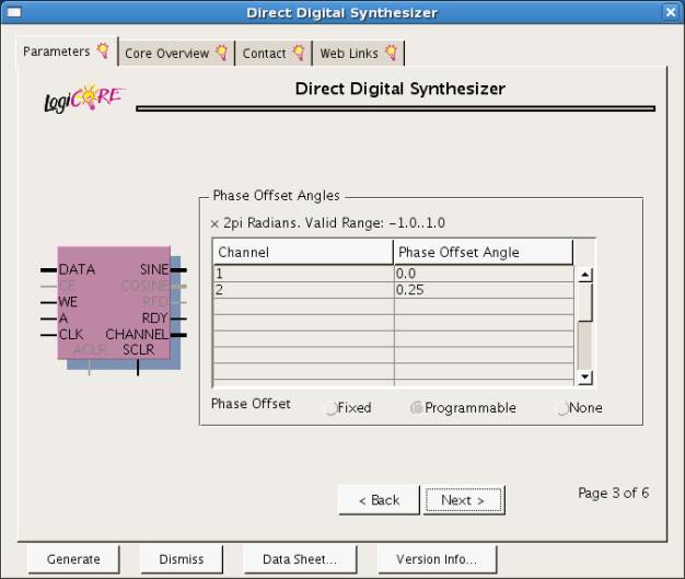
window (3/6) set initial phases of the channels (phases are entered in
radian/2π – e.g. 1.0 means 2π radian). Set the initial phase for the
channel 1 to: 0.0 and for the channel 2 to: 0.25 (i.e. π/2
radian).
Warning – due to a software bug it is difficult to see typed numbers. When
finally entered the value is displayed correctly.
Phase Offset set to: Programmable – you will be therefore allowed
to change the phase later in the system. The phase will be set using the slide
switches – load the value to the eight most significant bits of the
configuration word.
Then
click Next.
In this
window (4/6) you can set other properties of the DDS module.
Enable
option: Clear Options – SCLR Pin (this pin will be used for DDS reset
after changing the frequencies or phases and screen clearing by pressing the
BTN3 button) – this is synchronous reset.
Option Noise
Shaping leave in None position (this option is used for DDS algorithm modification to generate signal of
better quality).
Option Memory
Type set to Block ROM
In the
field Handshaking Options disable RFD Pin and enable Channel
Pin (defines the channel of the current sample).
Option Pipelined
should be disabled.
In the
field Accumulator Latency set option: One Cycle.
Then
click Next.
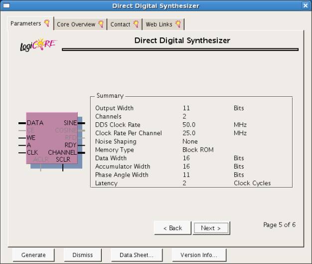
Summary
window (5/6) is presented. It is worth to remember additional information in
the summary of properties of designed component (Information field) and
the schematic diagram.
Then
click Next.
Second
summary window (6/6) is displayed.

Click Generate
button.
Now the
component generation starts – please wait a moment.
You
have to instantiate the component in your project using *.vho file (the
procedure is similar to that described earlier).
Circuit verification
The
circuit has to be verified experimentally by programming the FPGA on the
prototype board. You can also perform functional simulation if you need. After
the FPGA is programmed check the basic functionality of the system. Check the
Lissajous curves for different frequencies and phases. Remember to connect the VGA cable from the
VGA LCD display to the VGA output of the prototype board. Present the results
to the instructor. Explain why discrete structure (dots) of the curve is
sometimes visible.
Additional information about DDS:
http://en.wikipedia.org/wiki/Direct_digital_synthesizer
http://www.ieee.li/pdf/essay/dds.pdf
UCF file for the exercise, Digilent
Spartan-3 board, Spartan-3 3S200 FT256-4:
# Clock:
NET
"clk_i" LOC = "T9" ; # 50 MHz clock
# VGA
display:
NET
"rgb_o<1>" LOC = "R12" ; # R
NET
"rgb_o<2>" LOC = "T12" ; # G
NET
"rgb_o<0>" LOC = "R11" ; # B
NET
"hsync_o" LOC = "R9";
NET
"vsync_o" LOC = "T10";
# Slide
switches:
NET
"sw_i<0>" LOC = "F12" ; # active high when in UP
position
NET
"sw_i<1>" LOC = "G12" ; # active high when in UP position
NET
"sw_i<2>" LOC = "H14" ; # active high when in UP
position
NET
"sw_i<3>" LOC = "H13" ; # active high when in UP
position
NET
"sw_i<4>" LOC = "J14" ; # active high when in UP
position
NET
"sw_i<5>" LOC = "J13" ; # active high when in UP
position
NET
"sw_i<6>" LOC = "K14" ; # active high when in UP
position
NET
"sw_i<7>" LOC = "K13" ; # active high when in UP
position
#
Push-buttons:
NET
"btn_i<0>" LOC = "M13" ; # active high
NET
"btn_i<1>" LOC = "M14" ; # active high
NET
"btn_i<2>" LOC = "L13" ; # active high
NET
"btn_i<3>" LOC = "L14" ; # active high
#