Keyboard reading
Task: The circuit should read signals from the attached keyboard (in remote mode - emulated keyboard) and display the pressed keys on the 7-segment LED display (select any display from four available). As only a 7-segment display is available, only the following keys need to be recognized: 1,2,3,4,5,6,7,8,9,0,a,b,c,d,e,f. If any other key is pressed, the display should go blank.
Note: If the exercise is performed in the lab connect a USB keyboard to the USB HOST socket on the NEXYS A7 prototype board. There is a microcontroller on the board which converts HID USB communication into the PS/2 protocol - which we use in the exercise. In remote mode, we use a module of virtual buttons and switches. This module also allows you to emulate the PS/2 keyboard (Keyboard Mode in the "Virtual buttons"), so there is no need to connect a physical keyboard. A detailed description can be found in the manual for remote execution of laboratory tasks.
The BTNR (BTN3) button (rst_i signal) is an additional asynchronous reset (it should blank the display).
The signals "ps2_clk_i" and "ps2_data_i" are inputs of the PS/2 keyboard interface. Only reading from the keyboard should be performed (data and clock signals coming from the emulated keyboard should have the direction in defined). Detailed information on the operation of the PS/2 interface can be found in the link below:
Additional information - keyboard reading
Please note that the "ps2_clk_i" input cannot be used as a clock input and therefore cannot be connected to the clock inputs of the flip-flops. This input should be sampled like the data input (remember about the initial synchronization with the local clock).
Perform a functional simulation and verify the system practically by programming the test board.
Minimum simulation and verification requirements: Perform a simulation and verification on the prototype board by pressing the keys forming the index number of the student completing the exercise. In addition, the verification on the prototype board should also demonstrate all recognized numbers and letters and the reaction to other character (blanking). At the end of the verification, enter any number and show the operation of the asynchronous reset (rst_i). Clock frequency clk_i in the simulation - 100 MHz. Clock frequency ps2_clk_i in the simulation - 15 kHz.
Part
of the main (top level) VHDL design file with signal declaration:
entity top is
Port ( clk_i : in STD_LOGIC;
rst_i : in STD_LOGIC;
ps2_clk_i : in STD_LOGIC;
ps2_data_i : in STD_LOGIC;
led7_an_o : out STD_LOGIC_VECTOR (3 downto 0);
led7_seg_o : out STD_LOGIC_VECTOR (7 downto 0));
end top;
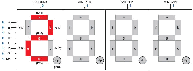
Fig. 1 Description of connections of individual display signals.
An example of displaying the digit '2'.
Design
constraints file for Nexys-A7 board (FPGA chip xc7a100tcsg324-1): iup8s.xdc
Design constraints file for remote mode (with support for virtual buttons and PS/2 keyboard emulation): iup8z.xdc