
Lab Home page
|
Department of Microelectronic Systems, Faculty of Electronics,
Telecommunications and Informatics, Gdansk University of Technology
|

|
Integrated Chipscope Analyzer
Task:
Using integrated logic analyzer Chipscope, test the unknown digital block
and specify its function.
For the unknown block Design Under Test (DUT) shown in Fig.1, only the following facts are known:
- it is a combinatorial circuit;
- it has 8-bit data input data_i (binary coded unsigned decimal);
- it has 8-bit data output data_o (binary coded unsigned decimal);
- it has 1-bit error output err_o(overflow);
- data on output data_o is a linear combination of input data: data_o = a*data_i + b,
where data_o and data_i are 8-bit unsigned decimal numbers, a and b are integer constants.
The goal is to find the values of a and b.
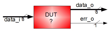
Fig. 1 DUT block
Procedure:
Create test environment for the tested block
First, the working environment for the block DUT has to be created. Generate test signal using
the 8-bit counter and connect it to the data input of DUT. The output data_o from DUT can
be connected to the LEDs, the error output can be connected to a single digit of 7-segment LED display
(the remaining digits can be dimmed; in case of other use of LED digits, modify ucf file
presented at the end of this page).
The proposed schematic diagram is shown in Fig. 2.
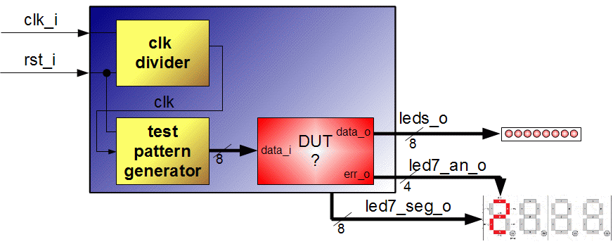
Fig. 2 The proposed block diagram for testing DUT
The DUT block is given as a synthesized netlist. The file
dut.ngc has to be included in the design in the following way:
- Declare the component dut in your VHDL code and then instantiate it.
- Copy the file dut.ngc to the main directory of your design.
The component declaration of this block is:
component dut is
port ( data_i : in STD_LOGIC_VECTOR (7 downto 0);
data_o : out STD_LOGIC_VECTOR (7 downto 0);
err_o : out STD_LOGIC);
end component;
Hardware verification of DUT operation using LEDs and slow clock
Implement the circuit from Fig. 2, setting the internal clock clk to low frequency (i.e. 1Hz).
Observe the LEDs and error signal on 7-segment display.
Insertion of logic analyzer into the circuit
Insert Chipscope analyzer to the circuit. The Chipscope analyzer consists of 2 blocks:
- integrated logic analyzer (ILA);
- integrated controller ICON (enables the connection of multiple logic analyzer blocks).
The Chipscope analyzer is inserted into the FPGA and it stores the observed signals
to the internal RAM. The Chipscope Analyzer software Analyzer (run on a PC), connects to the analyzer's
on-chip hardware using JTAG
and reads data stored in RAM. The read data is presented on the computer's screen.
The Chipscope analyzer has advanced trigger functions.
In this exercise, only basic functionalities are used.
Follow the procedure to insert Chipscope into your design:
-
Add new block to your project (this new block will be generated by the Coregenerator).
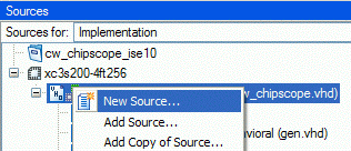
Fig. 3 Inserting new blocks
-
Select Source Type: IP (CORE Generator & Architecture Wizard) and enter the name.
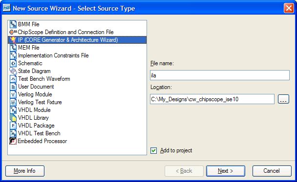
Fig. 4 Selecting the Coregenerator
-
In Coregenerator, select the block Debug&Verification/ChipscopePro/ILA (the newest version)
and set the following parameters:
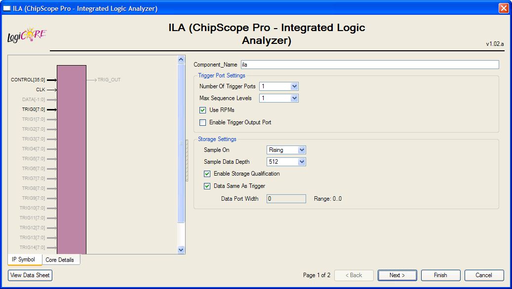
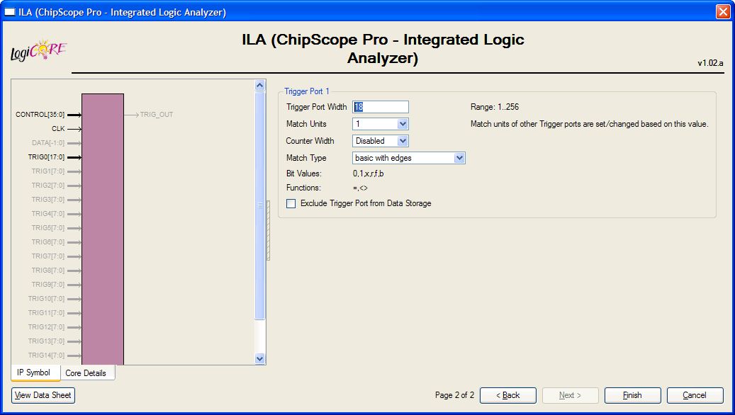
Fig. 5 Parameters of ILA block
-
Next, add chipscope_icon, also using Coregenerator,
selecting Debug&Verification/ChipscopePro/ICON (the newest version):
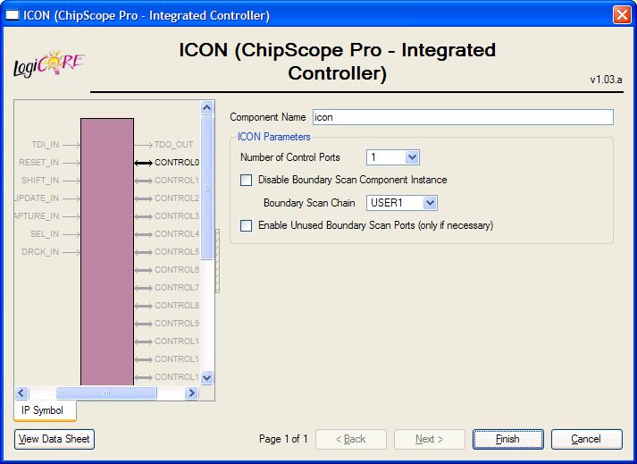
Fig. 6 Parameters of ICON block
-
Add the generated block to your design, according to the block diagram from Fig. 7 and
the following component declarations:
component icon
PORT (
CONTROL0 : INOUT STD_LOGIC_VECTOR(35 DOWNTO 0));
end component;
component ila
PORT (
CONTROL : INOUT STD_LOGIC_VECTOR(35 DOWNTO 0);
CLK : IN STD_LOGIC;
TRIG0 : IN STD_LOGIC_VECTOR(17 DOWNTO 0));
end component;
Increase the frequency of clk to a maximum. Observe the signals: data_i, data_o, err_o and rst_i.
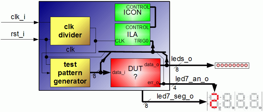
Fig.7 Schematic diagram showing the connection of the Chipscope
Working with the Chipscope analyzer software
After the implementation of the circuit with introduced ILA and ICON blocks, it is possible
to connect to the integrated analyzer from desktop computer using Chipscope Pro Analyzer
software.
At the beginning, after pressing  button, the software should detect the JTAG chain, as shown in Fig. 8, then click OK.
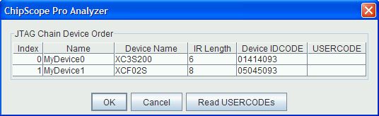
Fig. 8 Detected devices in JTAG chain
Group the observed signals into the buses (Fig.9) and give them the meaningful names as shown in Fig.10,
(right-click on the bus and seletct Rename).
For this project, it is advised to change the radix of the displayed bus signals (Bus Radix)
to Unsigned Decimal.
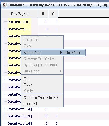
Fig. 9 Grouping the signals into a bus.
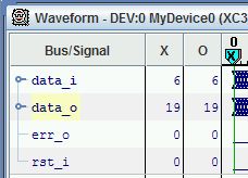
Fig. 10 Signals with the given meaningful names.
Now it is possible to set the trigger (when to start the data capture).
In this situation it is convenient to observe data starting from data_i=0.
The trigger setup is shown in Fig. 11. CAUTION: the zeros must be placed in the positions corresponding
to the equivalent bits of data_i. This can look different in your design!
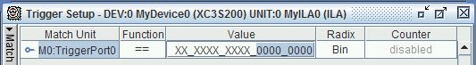
Fig. 11 Trigger setup
Run the analyzer: Trigger Setup/Run  .
If the trigger condition is detected inside the FPGA, the captured signals will be shown on the screen.
.
If the trigger condition is detected inside the FPGA, the captured signals will be shown on the screen.
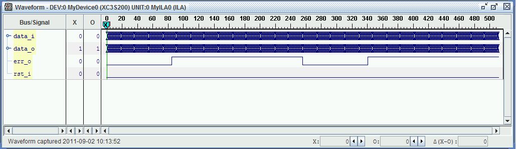
Fig. 12 Waveforms read by the Chipscope analyzer
Marker  shows the trigger time.
The beginning of the displayed data, in respect to trigger point, can be changed in Capture/Position.
To capture data without waiting for trigger, click: Trigger Setup/Trigger Immediate  .
.
UCF file, Digilent Spartan-3, Spartan-3 3S200 FT256-4:
#########################################################################################
# Clock:
NET "clk_i" LOC = "T9" ; # 50 MHz clock
#########################################################################################
# Push-buttons:
NET "rst_i" LOC = "L14" ; # pressed high BTN3
#########################################################################################
# LEDs:
NET "leds_o<0>" LOC = "K12" ; # high on
NET "leds_o<1>" LOC = "P14" ; # high on
NET "leds_o<2>" LOC = "L12" ; # high on
NET "leds_o<3>" LOC = "N14" ; # high on
NET "leds_o<4>" LOC = "P13" ; # high on
NET "leds_o<5>" LOC = "N12" ; # high on
NET "leds_o<6>" LOC = "P12" ; # high on
NET "leds_o<7>" LOC = "P11" ; # high on
#########################################################################################
# Seven-segment LED display:
NET "led7_an_o<3>" LOC = "E13" ; # leftmost digit, active low
NET "led7_an_o<2>" LOC = "F14" ; # active low
NET "led7_an_o<1>" LOC = "G14" ; # active low
NET "led7_an_o<0>" LOC = "d14" ; # rightmost digit, active low
#
NET "led7_seg_o<7>" LOC = "E14" ; # segment 'A', active low
NET "led7_seg_o<6>" LOC = "G13" ; # segment 'B', active low
NET "led7_seg_o<5>" LOC = "N15" ; # segment 'C', active low
NET "led7_seg_o<4>" LOC = "P15" ; # segment 'D', active low
NET "led7_seg_o<3>" LOC = "R16" ; # segment 'E', active low
NET "led7_seg_o<2>" LOC = "F13" ; # segment 'F', active low
NET "led7_seg_o<1>" LOC = "N16" ; # segment 'G', active low
NET "led7_seg_o<0>" LOC = "P16" ; # segment 'dp', active low
#########################################################################################
