Cascode amplifier
[PL]
- Design the cascode
amplifier shown in the figure for TSMC 0.35μm technology. The parameters of the amplifier are
given in the table and the version assignments can be found in the lista_aus file.
NOTE, transistor sizes can be varied with a step of λ=0.2μm,
with a minimum transistor size of W/L=3λ/2λ.
Assume the following transistor
parameters for the calculations: NMOS KP=94u VT0=0.55 GAMMA=0.6
LAMBDA=0.04; PMOS KP=33u VT0=-0.75 GAMMA=0.4 LAMBDA=0.06. The channel
length modulation factor LAMBDA actually depends on the channel length of
the transistor. To take this into account, use the LAMBDA values provided
in the file lambda-f(L).txt
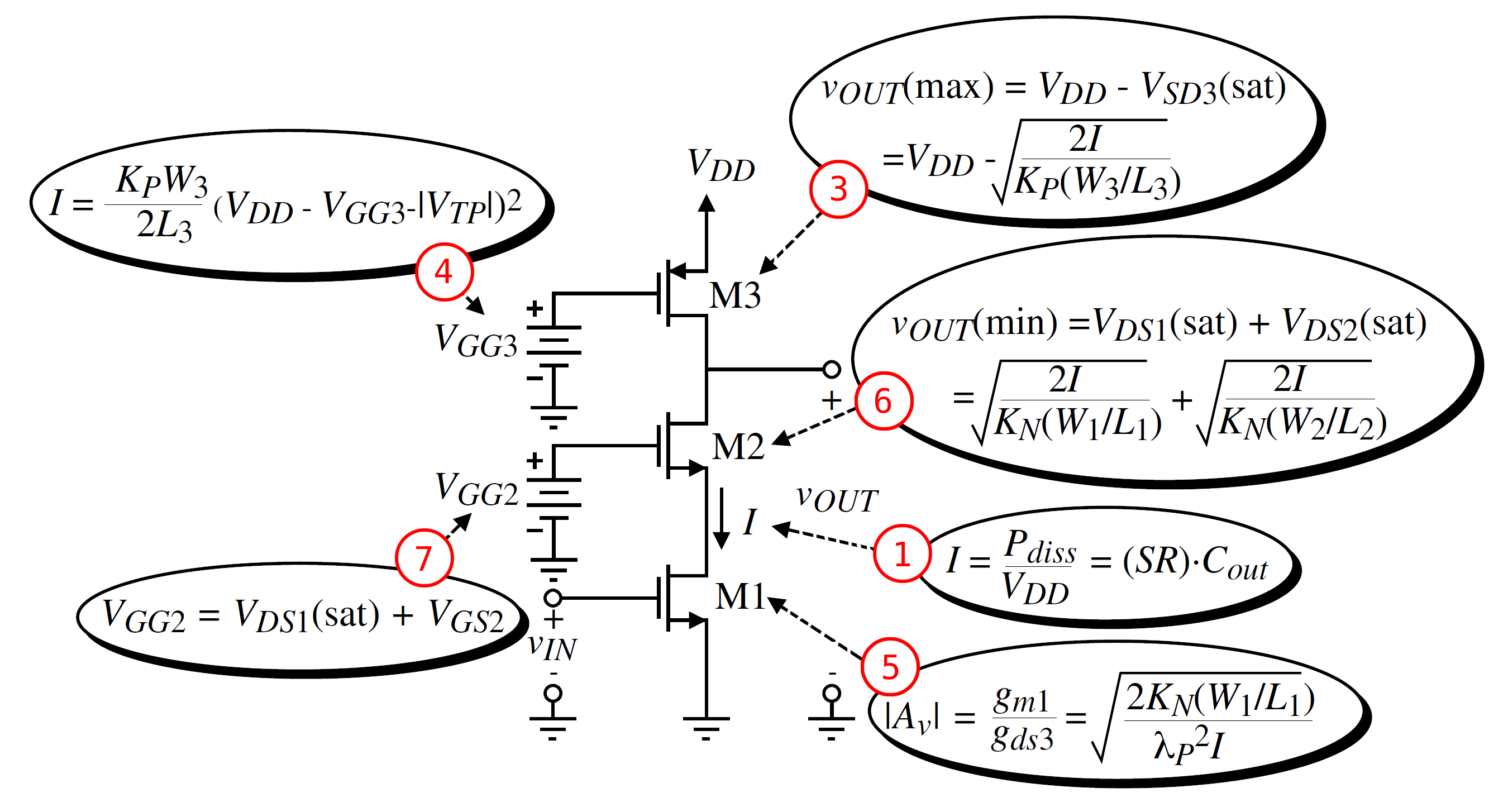
Design
procedure - determine sequentially taking into account the specified amplifier
parameter:
1) calculate amplifier bias current (Pdiss, SR)
2) choose the
channel length L ( the same for all transistors)
3) calculate W3/L3
(I i Voutmax)
4) calculate VGG3
5) calculate W1/L1
(Av, λ)
6) calculate W2/L2
(VDSsat2=Voutmin- VDSsat1)
7) calculate VGG2
8) calculate VIN
(DC voltage for bias gate of M1)
- Verify
the basic amplifier parameters by simulation using Spice MOS Level
1transistor model (Av, Voutmax, Voutmin, SR, Pdiss)
- Using
the simulator, optimise the amplifier for the
BSIM3 MOS model to meet the specified parameters. Report the following
amplifier parameters after optimisation: Av, Voutrange, SR, Rout, Pdiss, f3dB, GB.
- Present
the amplifier design in a report in doc, odt or
pdf format. The report should include a summary of the determined
parameters in a table and appropriate graphs, calculations and conclusions.The report should be accompanied by input
files to SPICE (cir).
- The
zipped report with attached files should be sent by email only. In the
subject line give: First name_Name_index
number_AUSlab_task3.
Parameters
of the cascode
amplifier:
|
Parameter |
Unit |
1 |
2 |
3 |
|
Av |
V/V |
50 |
50 |
50 |
|
Voutmax |
V |
2.5 |
2.8 |
2.5 |
|
Voutmin |
V |
1.0 |
1.0 |
0.8 |
|
CL |
pF |
8 |
4 |
4 |
|
SR |
V/μs |
12 |
12 |
12 |
|
Vdd |
V |
3.3 |
3.3 |
3.3 |
|
Pdiss< |
mW |
0.6 |
0.3 |
0.3 |