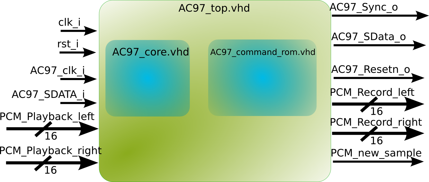
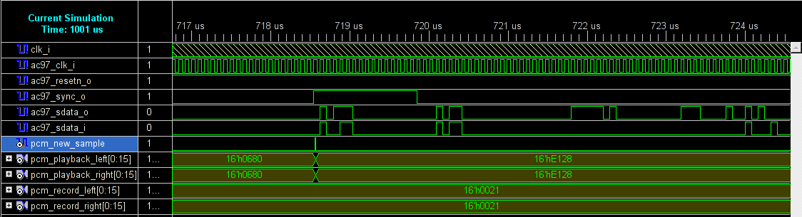
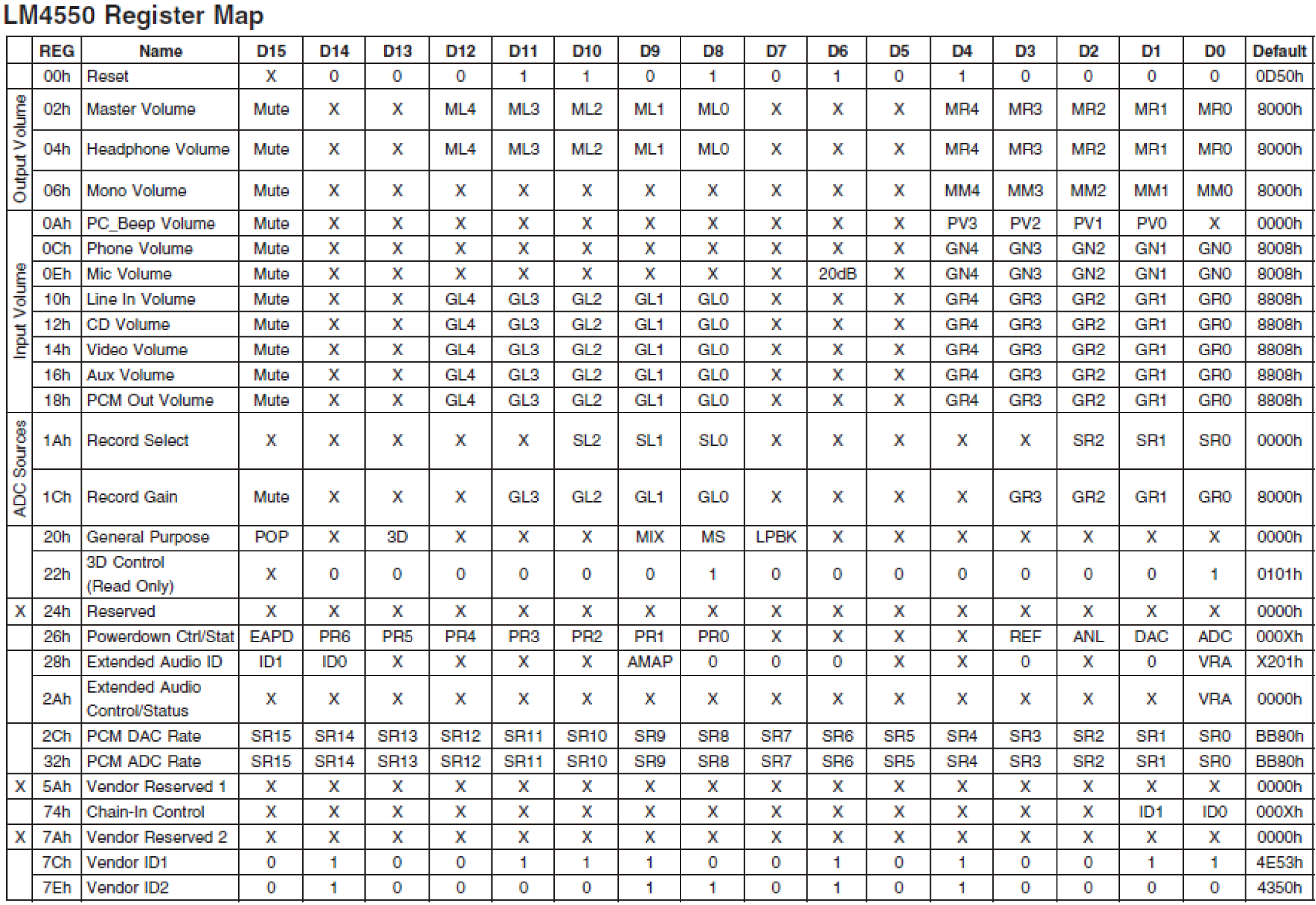
Tab. 1. Konfiguracja kodeka LM4550 zapisana w pamięci moduł AC97_command_rom.vhd
Adres
rejestru |
Wartość |
Znaczenie |
Opis rejestru |
| 0x00 |
0x0000 |
Reset kodeka LM4550 |
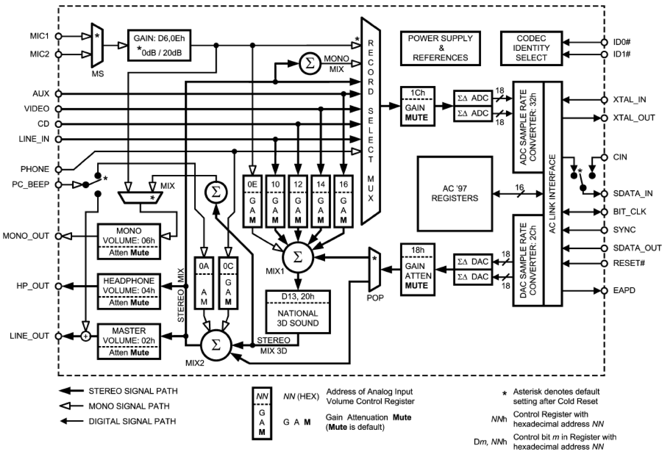
Writing any value to this register causes a Register Reset
which changes all registers back to their default values. If a
read is performed on this register, the LM4550 will return a
value of 0D50h.
This value can be interpreted in accordance
with the AC'97 specification to indicate that National 3D
Sound is implemented, 18-bit data is supported for both the
ADCs and DACs, and that headphone output is supported. |
0x02
0x04 |
0x0000 |
Wzmocnienie kanału Line Out/Amp Out
LCH -> 0dB
RCH -> 0dB
|
This output register allows the output level from either channel
of the stereo LINE_OUT to be muted or attenuated over
the range 0 dB - 46.5 dB in nominal 1.5 dB steps.
There are
5 bits of volume control for each channel and both stereo
channels can be individually attenuated.
The mute bit (D15)
acts simultaneously on both stereo channels of LINE_OUT. |
| 0x0E |
0x0040 |
Wzmocnienie bezpośredniego
przejścia Mic In
-> Line Out
(12dB+20dB)
|
These input registers adjust the volume levels into the stereo
mixers MIX1 and MIX2. Each channel may be adjusted over
a range of +12dB gain to 34.5dB attenuation in 1.5dB steps.
For stereo ports, volumes of the left and right channels can
be independently adjusted. Muting a given port is accomplished
by setting the MSB to 1. Setting the MSB to 1 for
stereo ports mutes both the left and right channels. The Mic
Volume register (0Eh) controls an additional 20dB boost for
the selected microphone input by setting the 20dB bit (bit
D6). |
| 0x18 |
0x0808 |
Wzmocnienie próbek PCM -> Line Out
(0dB)
|
These input registers adjust the volume levels into the stereo
mixers MIX1 and MIX2. Each channel may be adjusted over
a range of +12dB gain to 34.5dB attenuation in 1.5dB steps.
For stereo ports, volumes of the left and right channels can
be independently adjusted. Muting a given port is accomplished
by setting the MSB to 1. Setting the MSB to 1 for
stereo ports mutes both the left and right channels.
|
| 0x1A |
0x0000 |
Wybór źródła sygnału wejsciowego
dla przetworników ADC |
This register independently controls the sources for the right
and left channels of the stereo ADC. The default value of
0000h corresponds to selecting the (mono) Mic input for both
channels. |
| 0x1C |
0x0F0F |
Wzmocnienie rejestru nagrywania
22.5dB |
This register controls the input levels for both channels of the
stereo ADC. The inputs come from the Record Select Mux
and are selected via the Record Select Control register, 1Ah.
The gain of each channel can be individually programmed
from 0dB to +22.5dB in 1.5dB steps. Both channels can also
be muted by setting the MSB to 1. |
| 0x2A |
0x0001 |
Odblokowanie zmiany
częstotliwości próbkowania |
This read/write register provides status and control of the
variable sample rate capabilities in the LM4550. Setting the
LSB of this register to "1" enables Variable Rate Audio (VRA)
mode and allows DAC and ADC sample rates to be programmed
via registers 2Ch and 32h respectively. |
0x2C
0x32 |
0x0001 |
Zmiany częstotliwości próbkowania |
These read/write registers are used to set the sample rate
for the left and right channels of the DAC (PCM DAC Rate,
2Ch) and the ADC (PCM ADC Rate, 32h). When Variable
Rate Audio is enabled via bit 0 of the Extended Audio
Control/Status register (2Ah), the sample rates can be programmed,
in 1 Hz increments, to be any value from 4 kHz to
48 kHz. The value required is the hexadecimal representation
of the desired sample rate, e.g. 800010 = 1F40h. |