

Picoblaze 6 quick reference
CPU Features:
- Data: 8 bit.
- Instructions: 18 bit, each instruction executes in 2 clock cycles.
- Program address space: up to 4K instructions.
- 2 banks with 16 8-bit registers, marked: s0, s1, s2, ..., sF (no specialized accumulator, each register is an accumulator).
- 8-bit ALU unit (performs arithmetic operations on the register specified in the instruction, the result is entered into the same register, the second argument may be a constant value or another register).
- 64-byte scratchpad RAM
- ZERO and CARRY flags.
- A stack (31 items) for a CALL / RETURN operation
- 256 input ports (8-bit). Access to the port is possible through the 8-bit IN_PORT signal and the 8-bit port address PORT_ID. The READ_STROBE signal can be used to notify that the processor has read data from the port.
- 256 output ports (8-bit). Access to the port is possible through the 8-bit OUT_PORT signal and the 8-bit port address PORT_ID. The WRITE_STROBE signal is used to control a flip-flop that captures data from the output port.
- One interrupt input. The interrupt signal must be for 2 clock periods.
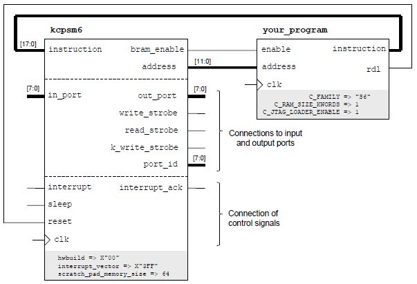
Embedding the processor in the VHDL code
The processor should be embedded inside the code along with the program memory (ROM) as shown in the figure below:
Selected processor instructions
Definitions:
"X" and "Y" represent processor registers s0, s1, ..., sF.
"kk" represents a constant value in the range 00 to FF.
"aa" represents an address from 00 to FF.
"pp" stands for a port address from 00 to FF.
Program control:
JUMP aa
JUMP Z,aa
JUMP NZ,aa
JUMP C,aa
JUMP NC,aa
CALL aa
CALL Z,aa
CALL NZ,aa
CALL C,aa
CALL NC,aa
RETURN
RETURN Z
RETURN NZ
RETURN C
RETURN NC
Logical operations:
LOAD sX,kk
AND sX,kk
OR sX,kk
XOR sX,kk
LOAD sX,sY
AND sX,sY
OR sX,sY
XOR sX,sY
Arithmetic operations:
ADD sX,kk
ADDCY sX,kk
SUB sX,kk
SUBCY sX,kk
ADD sX,sY
ADDCY sX,sY
SUB sX,sY
SUBCY sX,sY
Bit shifts:
SR0 sX
SR1 sX
SRX sX
SRA sX
RR sX
SL0 sX
SL1 sX
SLX sX
SLA sX
RL sX
I / O ports handling instructions:
INPUT sX,pp
INPUT sX,(sY)
OUTPUT sX,pp
OUTPUT sX,(sY)
Interrupt handling:
RETURNI ENABLE
RETURNI DISABLE
ENABLE INTERRUPT
DISABLE INTERRUPT
Comparison::
COMPARE statements perform subtraction but only change the ZERO and CARRY flags:
|
Flag |
Flag=0 when: |
Flag=1 when: |
|
ZERO |
arg1!=arg2 |
arg1==arg2 |
|
CARRY |
arg1>=arg2 |
arg1'<'arg2 |
COMPARE sX, kk
COMPARE sX, sY
The TEST instructions perform a bitwise AND operation between their arguments, then set only the ZERO and CARRY flags. Details in the Picoblaze processor manual.
TEST sX, kk
TEST sX, sY
Assembler
The assembler converts the program code into RAM memory described as a module in VHDL language. Such memory is instantiated together with the processor. Each time the program is changed in the assembly language, it is necessary to run the assembler program, and then re-implement it into the FPGA.
Running an assembler program:
kcpsm6.exe <software>.psm
The assembler enables, among others:
· Using labels when jumping
· Defining constants (CONSTANT command)
· Entering own register names (NAMEREG command)
Procedure for using the Picoblaze processor
- See the documentation for the Picoblaze processor.
- Unpack the Picoblaze and Assembler files.
- Upload the kcpsm6.exe and ROM_form_templates\ROM_form_7S_2K_14March13.vhd files to the selected folder (it can be a folder with Vivado source files, you will not need to copy the resulting files after assembly).
- Write the program in assembly language (e.g. my_software.psm) and perform its assembly (e.g. in the same folder as kcpsm6.exe): kcpsm6.exe my_software.psm
- In the project described with the VHDL language (e.g. my_hardware.vhd), the Picoblaze processor (the kcpsm6.vhd file from the unpacked package) should be embedded.
- As a result of assembly, we will get the VHDL my_software.vhd file with program memory.
- The program memory should be embedded in the project and connected to the processor and clock.
- Carry out the implementation.
Additional information

This document is based on materials and application notes from Xilinx.