CMOS cascode operational amplifier
simulation tests and layout
design
Exercise 2 consists of two parts:
·
simulation tests of a cascode operational amplifier,
·
designing the topography of the amplifier, extracting the schematic from
the topography design and verifying its parameters.
Before performing the task, it is necessary to repeat
the knowledge about operational amplifiers and operation of PSPICE simulator
and MAGIC topography editor.
Figure 1 shows the schematic of an operational cascode
amplifier designed for 0.5um AMI technology. The supply voltage Vdd of the
amplifier is 3.3 V, and the input common voltage is Vdd/2. The bias voltage VB1
should be selected so that the biasing current of the differential pair (IDM9)
is 10uA - for students with even index
number and 20uA - odd index number. Select the bias voltage VB2 to obtain the
largest range of output voltage. Please explain your choice in the report. You
should also propose and implement a modification of the amplifier's schematic
that improves the output voltage range.
In the first part of the exercise simulate the
amplifier loaded with CL=4pF and determine:
- operating points of transistors and power
dissipation Pdiss of the amplifier,
- offset voltage of the amplifier,
- the characteristics of the voltage gain in the open
feedback loop, read Avo, GB, PM,
- range of variation of input common voltage ICMR,
- output voltage swing Voutswing,
- slew rate of output voltage,
- CMRR and PSRR,
- input capacitance Cin, output resistance Rout.
Using Monte
Carlo analysis, investigate the effect of the mismatch of transistor parameters
on the input offset voltage Vioff,
amplifier DC gain Avo and CMRR. For this purpose, assume that MOS transistors
have a 0.5% variation in threshold voltage and transconductance coefficient (in
MOS transistor models, add the parameter DEV=0.5% to VTH0 and TOX)
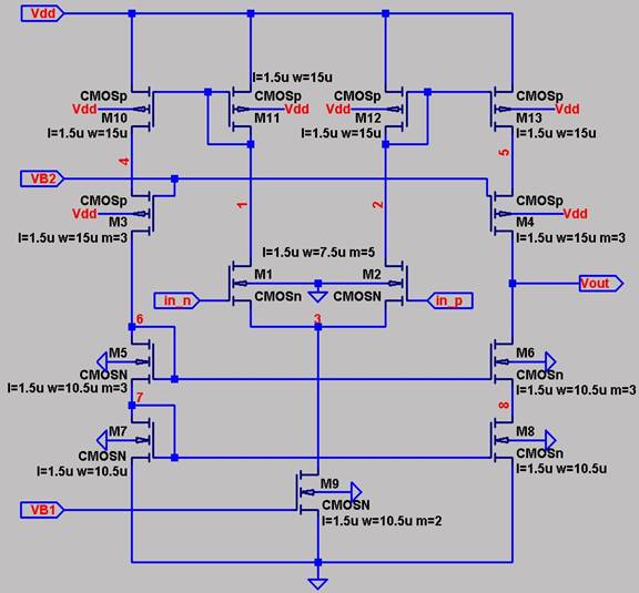
Fig. 1 Cascode operational
amplifier
In the second part of the exercise, design the layout
of the amplifier using MAGIC using the following transistor placement:
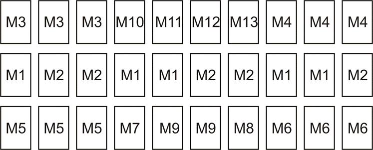
Fig. 2 Cascode amplifier transistor
placement.
Then extract the amplifier schematic from the
topography design and perform simulation tests.
For the exercise, prepare a report in doc, odt or pdf
format according to the attached template. The report should include a summary
of the determined parameters in a table and the corresponding graphs,
calculations and conclusions. Files for SPICE simulator (cir) and topography
projects (mag) should be attached to the report. NOTE: each simulation should
be accompanied by the corresponding file ready to run! Zipped reports with
attached files should be sent only by email, in the subject of the email give:
Name_Name_index number_AUSLAB_year_task2.
the template for the report:: doc