

Lab 1: Creating hardware platform for freeRTOS and running demo software
Contents
Step 1: Creating the Hardware Project
Step 2: Creating Block diagram of the microprocessor system
Step 3: Synthesis and implementation of the hardware
Step 4: Analyzing the Created Project
Step 5: Exporting the hardware to SDK
Step 6: Creating new application in Xilinx SDK
Step 7: Examine the files and projects in your system
Step 9: Run single thread with simple floating-point computation and printout
Setup
For this lab, you will need a Xilinx Zybo Z7-20 FPGA Board and a USB cable. Connect the USB cable to the PC and the Zybo Z7-20 board to connector PROG/UART. With this cable, the programming of the FPGA will be done, as well as serial communication between the board and PC.
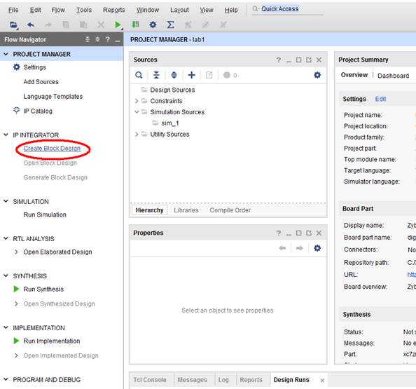
Step 1: Creating the Hardware Project
1. Run Vivado ![]() from desktop or menu: All Apps/Xilinx Design Tools Vivado 2018.3.
from desktop or menu: All Apps/Xilinx Design Tools Vivado 2018.3.
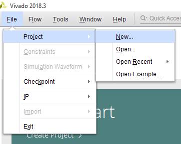
2. In Vivado create new project (File/Project/New):
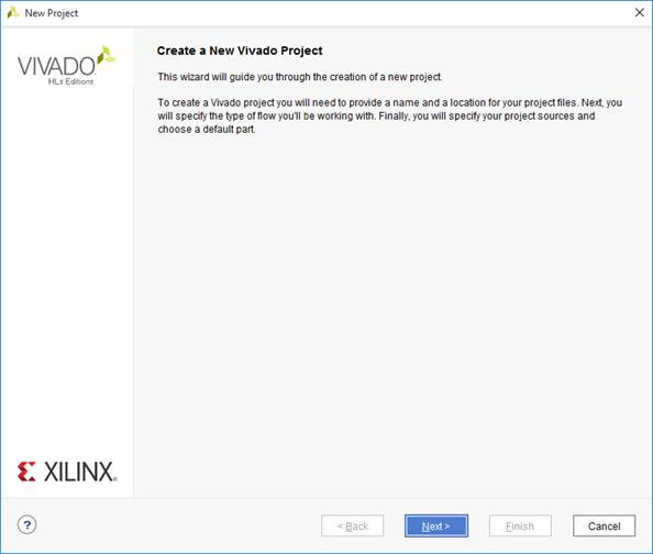
New window will open with New Project wizard:
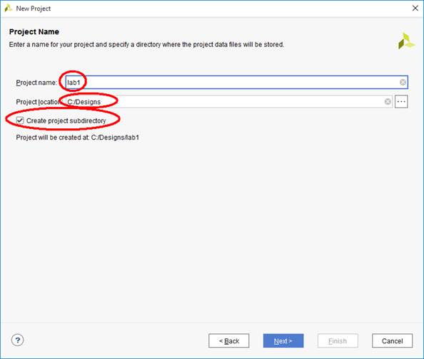
3. Enter the name of your project. The Project location should contain the directory where you are allowed to write (for example C:\Designs) and make sure that Create project subdirectory checkbox is selected, because software will create the directory of the same name as your design name and all the design files will be placed in this folder.
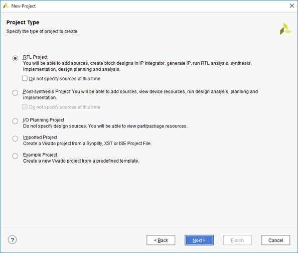
In Project Type window, select RTL Project:
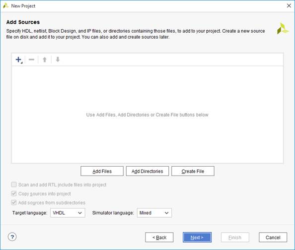
4. In Add Sources you can select your preferred HDL language (Target language). You will not add any files here, so click Next:
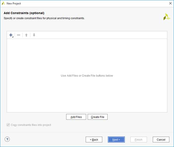
5. In the next window you will also do not add any constraints, so click Next. The constraints can be added later, if needed.
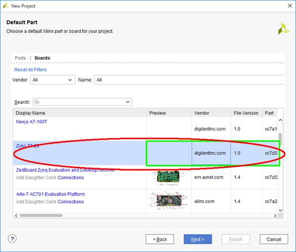
6. In Default Part, first switch from Parts view to Boards view, then select the line with Zybo Z7-20. Do not click directly on blue text “Zybo Z7-20” because it is a link which will open in a browser, but click anywhere to the right on this line (green rectangle on the picture). Finally click Next.
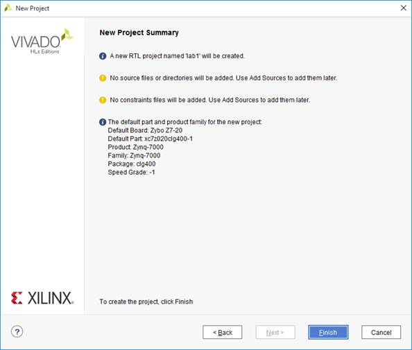
7. The last screen of this wizard presents the summary. Just click Finish.
Step 2: Creating Block diagram of the microprocessor system
1. Having created the empty project, now you will add the microprocessor system using block diagram design entry method. This will be done with IP INTEGRATOR flow by creating Block Design. Click Create Block Design:
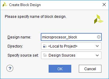
2. In the next window you can set the name of the block design, do not change anything else. Press OK and wait for creating new block diagram.
3. Now add the following new blocks using +
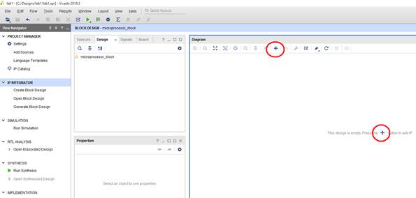 and searching for the appropriate block names:
· ZYNQ7 Processing System
· AXI Timer
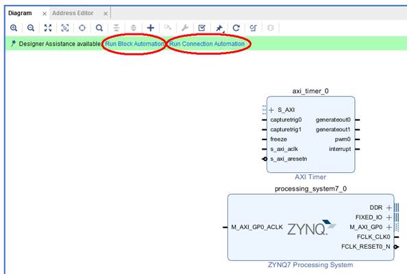
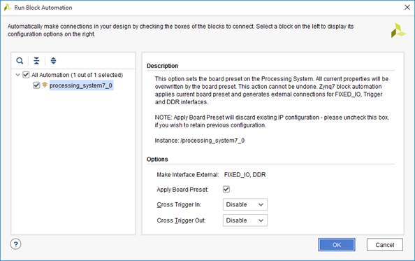
4. When finished, click ![]() to regenerate the diagram, then click Run Block Automation Wizard, which will help you to configure the MicroBlaze subsystem
to regenerate the diagram, then click Run Block Automation Wizard, which will help you to configure the MicroBlaze subsystem
Block Automation will ask you about the basic parameters of the Zynq subsystem, do not change anything, just click OK:
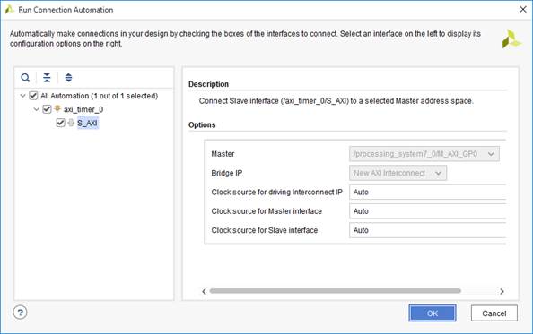
5. When Block Automation finishes, start the Connection Automation Wizard with default settings:
6. Now the clock diagram is ready, it should look like this:
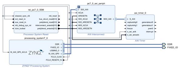
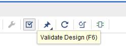
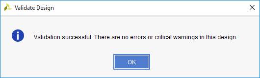
You can validate your block diagram using button Validate Design (F6):
The block design should have no errors:
Step 3: Synthesis and implementation of the hardware
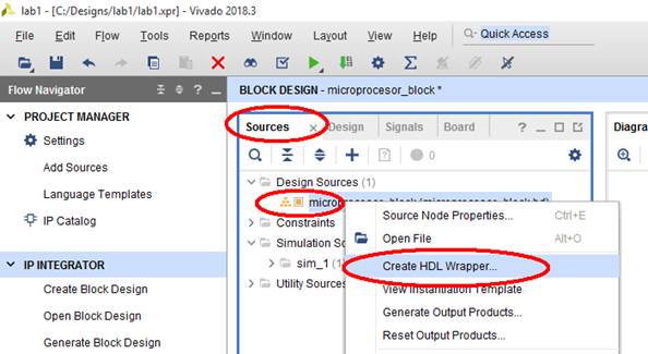
1. Your block design is now a part of the design sources, you can see it in the Sources tab. To use such a block diagram in the implementation flow, you need to wrap it in HDL block. This can be done with the Create HDL Wrapper command:
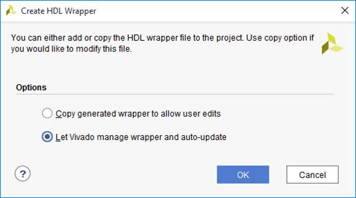
Let Vivado manage the updates of the HDL file and click OK:
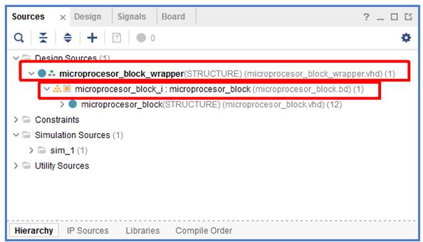
2. Now in the Sources tab you will see another level of the hierarchy in your project: the block design in instantiated inside HDL file:
3. The hardware is ready and you can synthesize and implement it. It is enough to click Generate Bitstream, the under hood make will automatically check which operations need to be done:
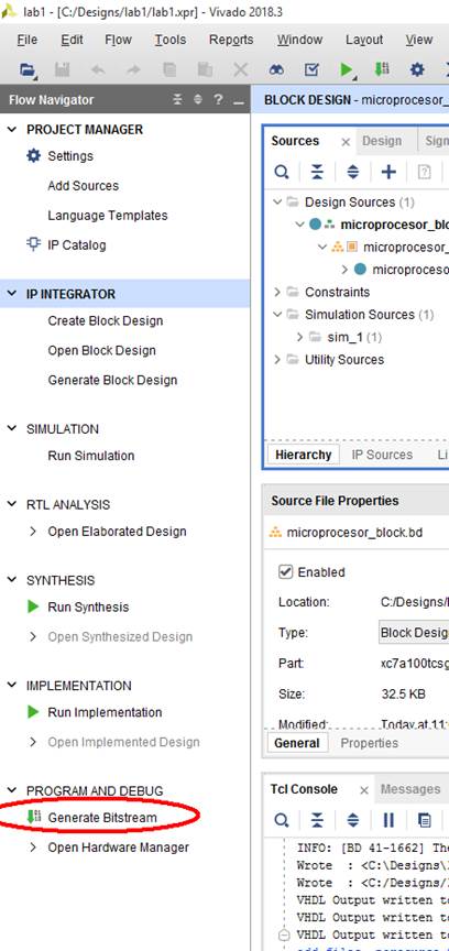
4. After several minutes your hardware will be synthesized and implemented, the bitstream file containing the FPGA hardware configuration will be created. The current status of Vivado is presented in top-right corner of the screen:
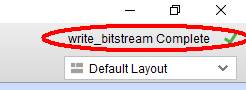
You can also look at Deign Runs window at the bottom.
When you see write_bitstream Complete message, your hardware is now ready, but you need to create software. This will be done in another tool called SDK.
Step 4: Analyzing the Created Project
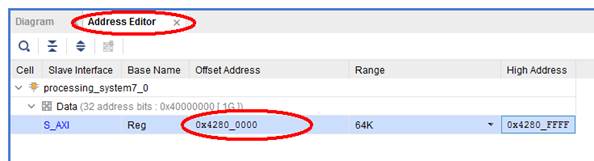
Before you start writing the software, you need to know the technical parameters of your hardware, such as addresses, blocks’ parameters, etc.
1. In the Address Editor tab, you can see the addresses assigned to S_AXI slave port:
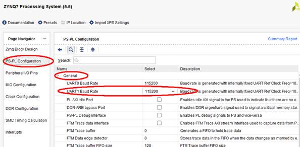
2. In the block diagran, double click on Zynq7 Processing System and note, which UART is activated:
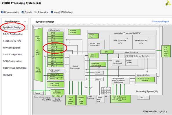
also remember the transmission speed of this port:
Step 5: Exporting the hardware to SDK
Having your hardware ready, you need to create software. This is done in another tool called Xilinx SDK. First you have to export your hardware from Vivado to Xilinx SDK.
3. In Vivado you will export your design and launch Xilinx SDK with the following commands:
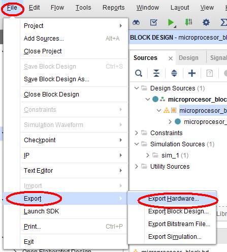
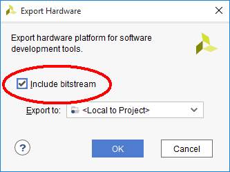
Do not forget to select the include the bitstream in the exported platform:
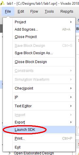
4. Finally you launch Xilinx SDK to start creating the software:
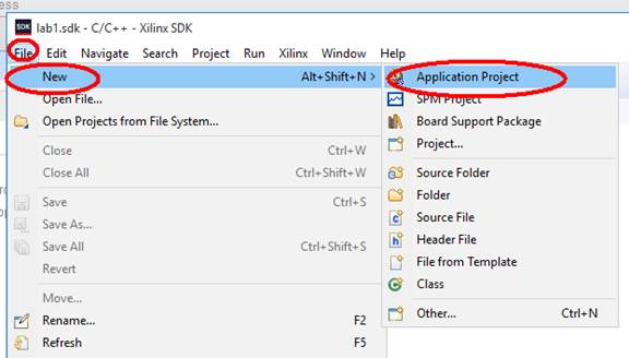
Step 6: Creating new application in Xilinx SDK
Xilinx SDK opens with already created hardware platform imported from Vivado. Hardware platform contains information about the hardware resources needed by the software, such as the number and types of microprocessors, the list of peripheral devices and the addresses of their registers. Whenever you change the hardware in Vivado, the hardware platform should be updated.
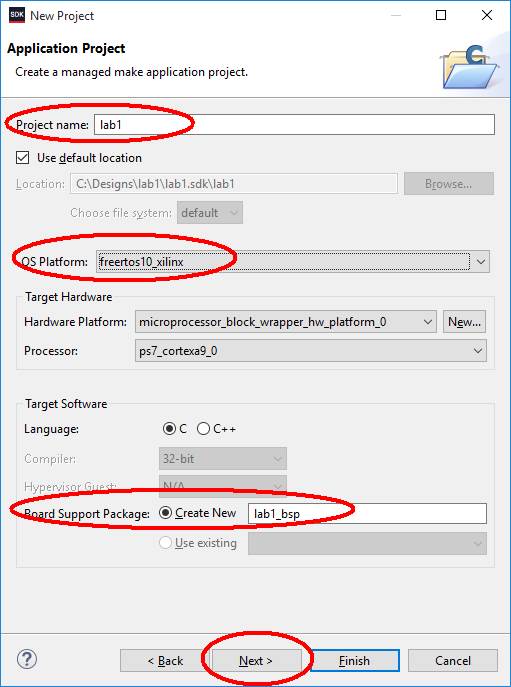
5. Create new application project from menu File/New/Application project:
Enter the name of your application. You should also let the software to create new Board Support Package (BSP) for this platform. BSP is a set of software which is dedicated for a given hardware platform and is used by application (it is the software that mediates between your application and the hardware). BSP contains the drivers for hardware devices, their addresses and parameters which can be easily used by applications:
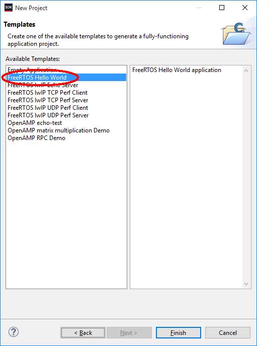
Then you ask for creation of template project containing tests for the peripheral devices available in the system and click Finish:
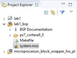
Step 7: Examine the files and projects in your system
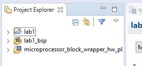
Your environment in SDK should now contain three projects:
- Hardware platform ![]()
- Board Support Package ![]()
- User C application ![]()
1. First examine the files in the hardware platform, open *.hdf file and see what is inside.
2. Then examine BSP project. In system.mss you will find software settings for your application:
· the operating system used (or standalone);
· which device will be used for stdin and stdout (for standalone);
· drivers for hardware blocks;
· compiler flags and settings.
In the folder ps7_cortexa9_0/include there are all include files.
First take a look at xil_types.h – there are defined types of variables you should use in your application: for example u32, u8.
Another important file is xparameters.h which contains macros with the addresses and parameters of your hardware. When writing your software, you should not use the numerical addresses but macros from this file. When the hardware changes, the addresses can also change, but all the changes will be automatically included in xparameters.h. Therefore, if you use the macros from xparameters.h, you do not need to track the changes in hardware.
In ps7_cortexa9_0/libsrc there are many folders with the drivers – if you want to use a hardware peripheral block in your software, you need to look at those files to see which driver functions are available and how to use them.
3. Finally take a look at application project. In src subdirectory there are all *.c and *.h files that make you your application:
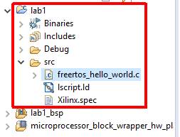
In our example, in the file freertos_hello_world.c there is main() function. Please take a look at it, so you will know what happens when you run the software.
Step 8: Run test application
Before you start running the applications, you need to “produce” the hardware. The bitstream file containing the configuration of your hardware has been generated in Vivado during the first part of this lab. Now you have to send this file to FPGA to program it.
If you have problems with programming and you cannot manually reset the board (remote lab), check this document: Remote reset by JTAG.
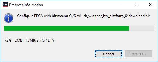
1. Click on the following button to send bitstream file by the JTAG programmer, which is connected to the PC by USB cable:

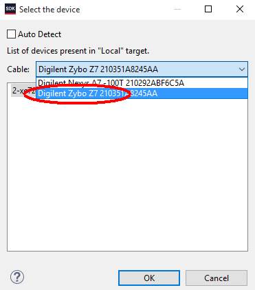
If you have more than one board connected to your PC, it could be necessary to select which board to program:
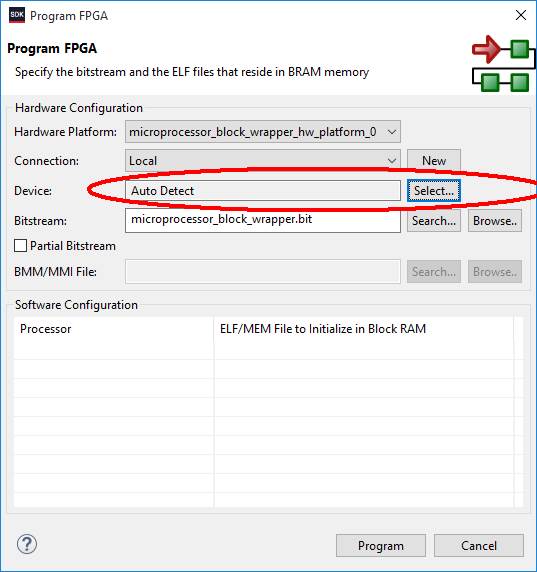
In the next window you can decide not to use auto detection, but specifically decide which device will be programmed (xc7z020):
After several seconds you should see the programming progress:
More information you will find here: Working with multiple FPGAs connected to the PC
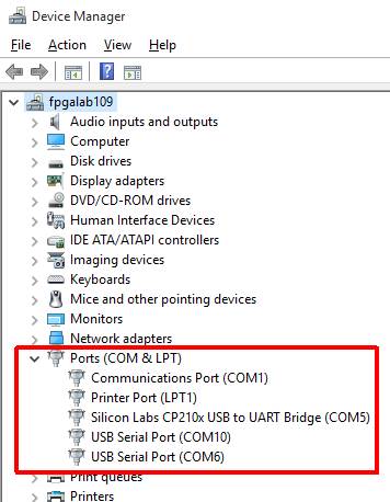
2. Now you need to determine the serial port number of your FPGA board connected by USB. In Windows open the Device Manager:
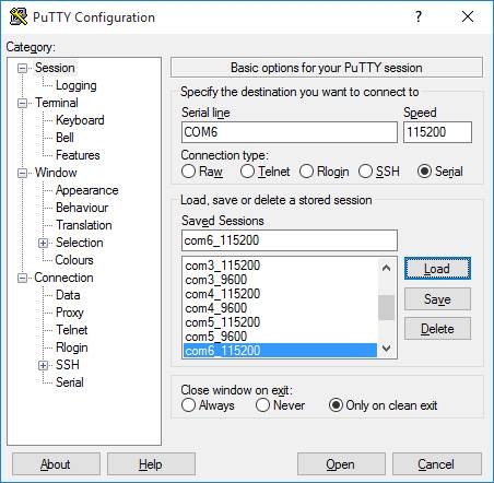
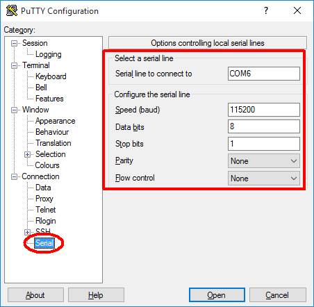
3. Run serial port terminal, for example putty in Windows and configure it for serial configuration. You need to specify the serial port number and the serial transmission parameters such as speed, number of data or parity bits and handshaking method. Those settings must be the same as used by your hardware block – you can check them in Vivado.
For example, putty settings are presented below, assuming COM10:
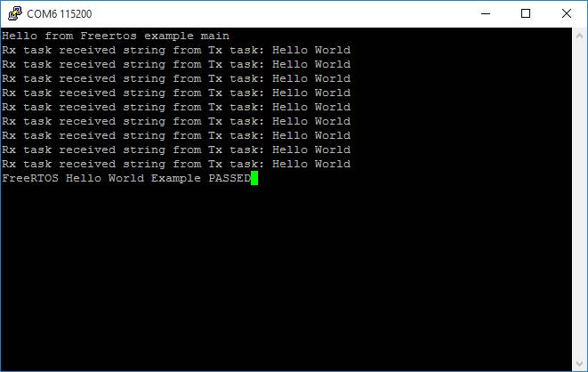
Now you will see the serial port terminal window connected to your microelectronic system on your PC. So it is the time to run the software.
4. Right-click on your application project and select Run As/Launch on hardware:
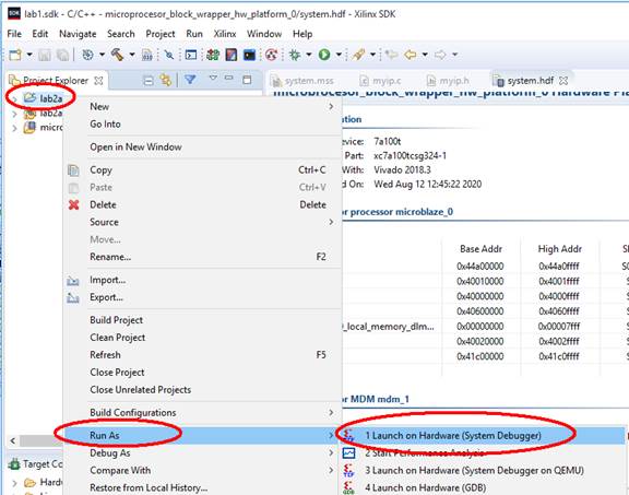
You probably will need to create your own launch configuration. More information about launching the software you will find here: Working with multiple FPGAs connected to the PC
The SDK will use built-in debugger to send the application code to the memory and execute it. You should see the application output:
Step 9: Run single thread with simple floating-point computation and printout
Create a single task, perform arbitraty floating-point calculation and printout the result to the serial console. Remeber, to read the information regarding floating point operations and printing on the console.
Change history
Adding Step 9: M.W. (09/2023)
Adaptation to version Vivado 2018.3: M. Wójcikowski (08/2020).