

Lab 1: Simple Hardware Design
This text is based on teaching materials from Xilinx (www.xilinx.com).
Contents
Step 1: Creating the Hardware Project
Step 2: Creating Block diagram of the microprocessor system
Step 3: Synthesis and implementation of the hardware
Step 4: Analyzing the Created Project
Results required to complete the exercise
Introduction
This lab guides you through the process of using CAD software Vivado 2018.3 to create a hardware of a simple processor system. After completing this lab, you will be able to create a hardware consisting of MicroBlaze processor and basic IP (Intellectual Property) blocks available in Xilinx library.
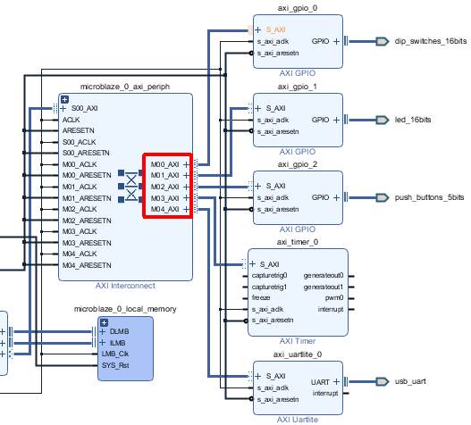
The purpose of the lab exercises is to walk you through a complete hardware and software processor system design. Each lab will build upon the previous lab. The following diagram represents the completed design:
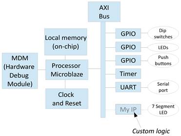
In this lab, you will create a processor system consisting of the following processor IP:
· MicroBlaze processor
· Local memory with BRAM and LMB bus and LMB controller
· AXI bus
· MDM (MicroBlaze Debug Module)
· UART
· GPIO for DIP switches, push buttons and LEDs
This lab comprises the following primary steps: you will create a hardware project in Vivado, analyze the project created and generate the processor system bitstream. Below each general instruction for a given procedure, you will find accompanying step-by-step directions and illustrated figures providing more detail for performing the general instruction.
Step 1: Creating the Hardware Project
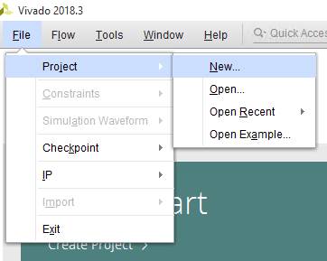
1. Run Vivado ![]() from desktop or menu: All Apps/Xilinx Design Tools Vivado 2018.3.
from desktop or menu: All Apps/Xilinx Design Tools Vivado 2018.3.
2. In Vivado create new project (File/Project/New):
New window will open with New Project wizard:
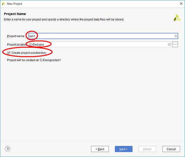
3. Enter the name of your project. The Project location should contain the directory where you are allowed to write (for example C:\Designs) and make sure that Create project subdirectory checkbox is selected, because software will create the directory of the same name as your design name and all the design files will be placed in this folder.
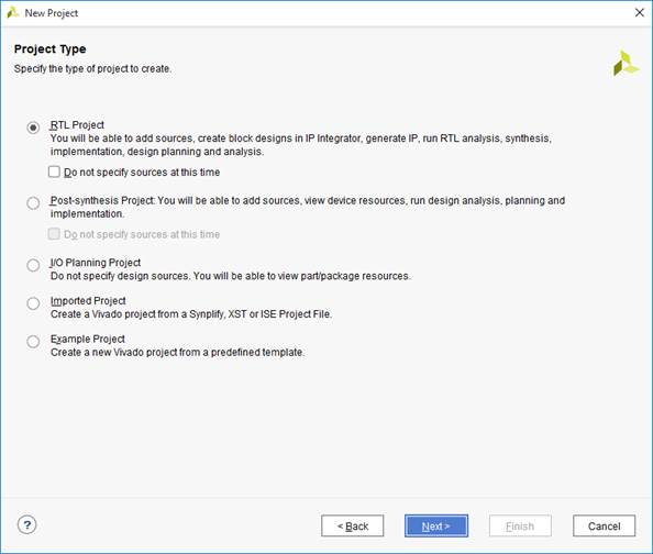
In Project Type window, select RTL Project:
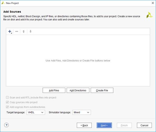
4. In Add Sources you can select your preferred HDL language (Target language). You will not add any files here, so click Next:
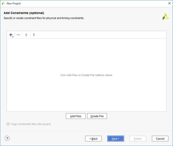
5. In the next window you will also do not add any constraints, so click Next. The constraints can be added later, if needed.
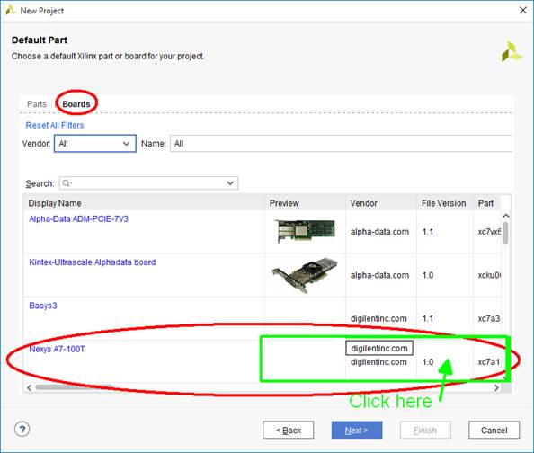
6. In Default Part, first switch from Parts view to Boards view, then select the line with Nexys A7 100T. Do not click directly on blue text “Nexys A7 100T” because it is a link which will open in a browser, but click anywhere to the right on this line (green rectangle on the picture). Finally click Next.
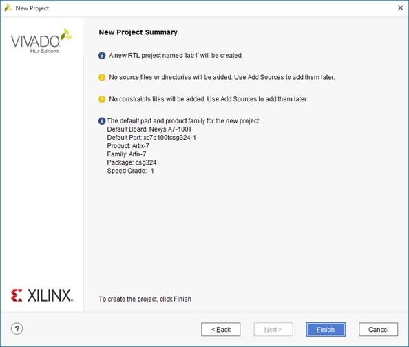
7. The last screen of this wizard presents the summary. Just click Finish.
Step 2: Creating Block diagram of the microprocessor system
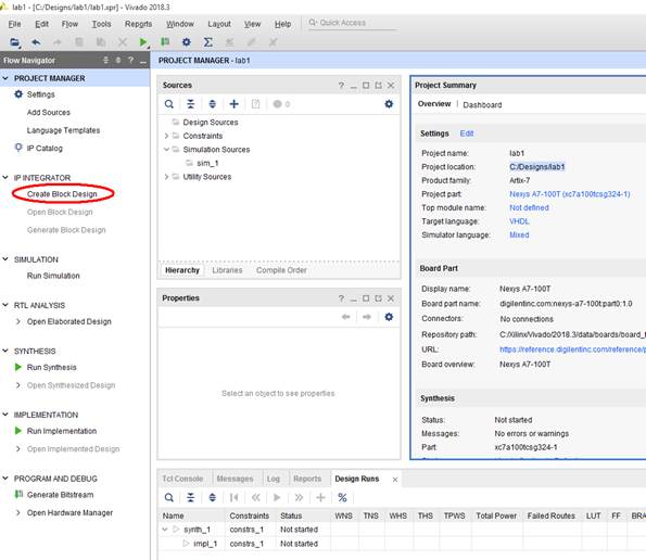
1. Having created the empty project, now you will add the microprocessor system using block diagram design entry method. This will be done with IP INTEGRATOR flow by creating Block Design. Click Create Block Design:
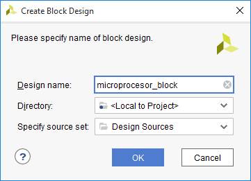
2. In the next window you can set the name of the block design, do not change anything else. Press OK and wait for creating new block diagram.
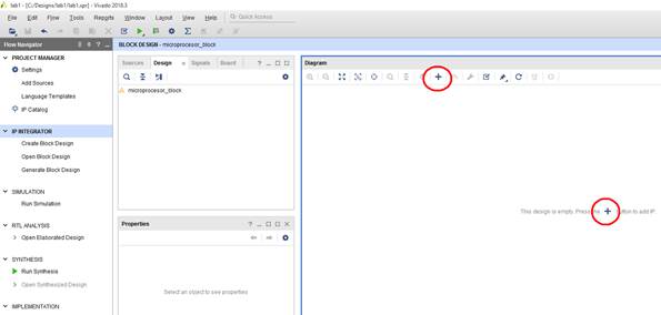
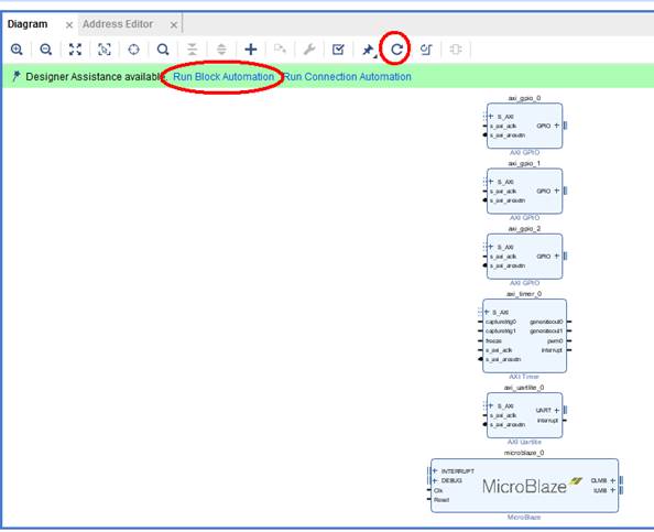
3. Now add the following new blocks using +
 and searching for the appropriate block names:
· MicroBlaze
· AXI GPIO (3 instances)
· AXI Timer
· AXI Uartlite
4. When finished, click ![]() to regenerate the diagram, then click Run Block Automation Wizard, which will help you to configure the MicroBlaze subsystem
to regenerate the diagram, then click Run Block Automation Wizard, which will help you to configure the MicroBlaze subsystem
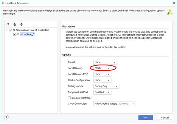
Block Automation will ask you about the basic parameters of the MicroBlaze subsystem, change only Local Memory to 32KB and click OK:
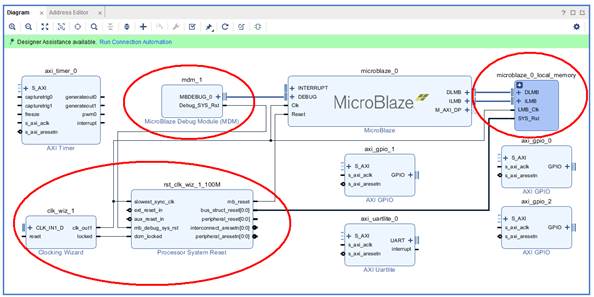
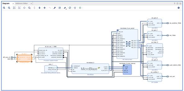
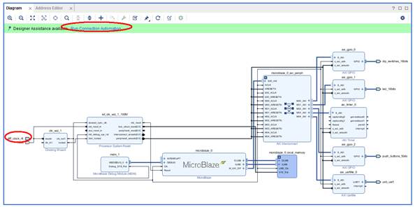
5. When Block Automation finishes, click ![]() again to regenerate the schematic diagram. Now you can see, that the new blocks have been added: memory, mdm, clock, reset and connected to microprocessor. The other blocks are not yet connected, but you will do this with the help of Connection Automation wizard.
again to regenerate the schematic diagram. Now you can see, that the new blocks have been added: memory, mdm, clock, reset and connected to microprocessor. The other blocks are not yet connected, but you will do this with the help of Connection Automation wizard.
6. Now start the Connection Automation Wizard:
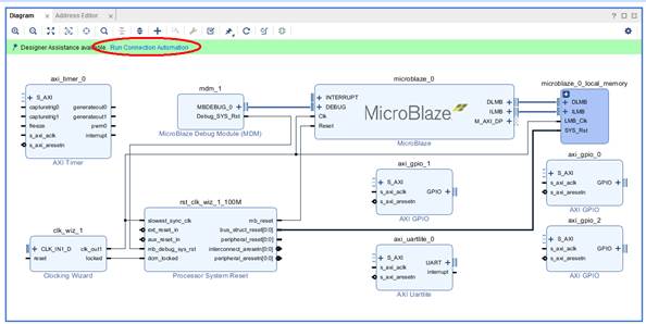
In the left panel, select all checkboxes:
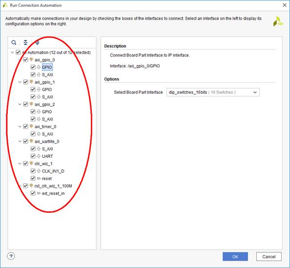
then set the parameters of each block:
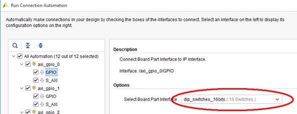
The wizard is aware of the hardware, because you selected the Nexys board in one of the earlier steps. Set the following parameters:
· axi_gpio_0/GPIO: dip_switches_16 bits (16 Switches)
· axi_gpio_1/GPIO: led_16 bits (16 LEDs)
· axi_gpio_2/GPIO: pusch_buttons_5bits (5 Push Buttons)
· axi_uartlite_0/UART: usb_uart (USB UART)
The others settings remain unchanged.
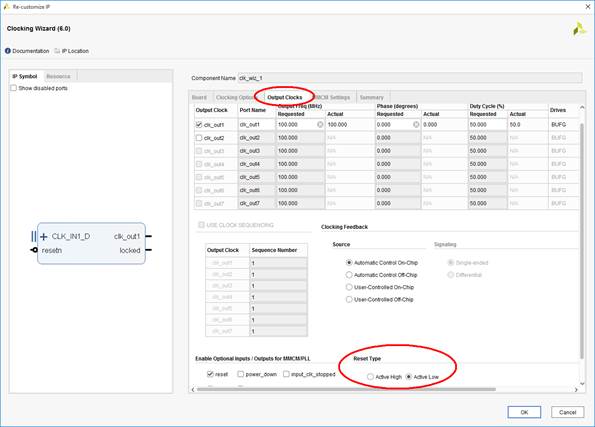
7. Now double-click on the block clk_wiz_1 (click in the center on the block, not on the port names):
The clocking wizard will open, where you will change the primary clock from differential to single-ended:
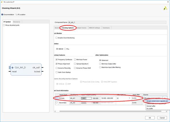
and the polarization of reset signal to Active Low:
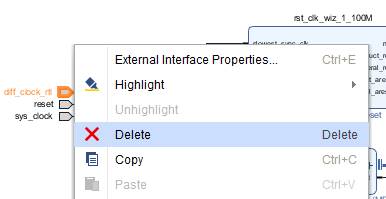
8. Because you changed the block pins (clock from differential to single-ended) and the polarization of the reset, you need to run the Connection Wizard once again with the default settings. You also need to delete the unused port diff_clock_rtl by right-clicking on it:
9. Now the clock diagram is ready, it should look like this:
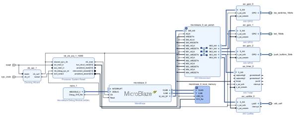
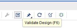
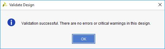
You can validate your block diagram using button Validate Design (F6):
The block design should have no errors:
Step 3: Synthesis and implementation of the hardware
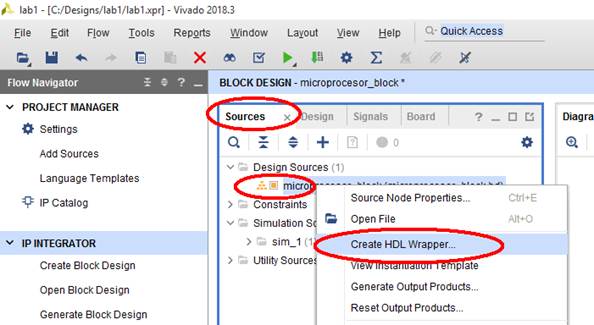
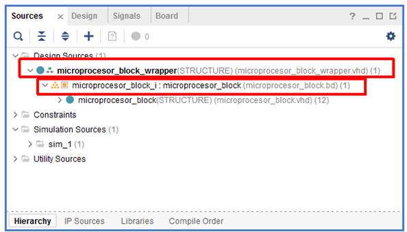
1. Your block design is now a part of the design sources, you can see it in the Sources tab. To use such a block diagram in the implementation flow, you need to wrap it in HDL block. This can be done with the Create HDL Wrapper command:
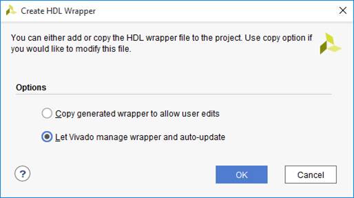
Let Vivado manage the updates of the HDL file and click OK:
2. Now in the Sources tab you will see another level of the hierarchy in your project: the block design in instantiated inside HDL file:
3. The hardware is ready and you can synthesize and implement it. It is enough to click Generate Bitstream, the under hood make will automatically check which operations need to be done:
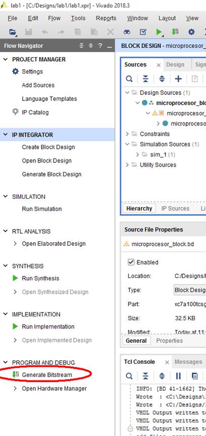
4. After several minutes your hardware will be synthesized and implemented, the bitstream file containing the FPGA hardware configuration will be created. The current status of Vivado is presented in top-right corner of the screen:
You can also look at Deign Runs window at the bottom.
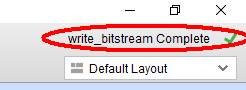
When you see write_bitstream Complete message, your hardware is now ready, but you need to create software. This will be done in another tool called SDK.
Step 4: Analyzing the Created Project
Before you start writing the software, you need to know the technical parameters of your hardware, such as addresses, blocks’ parameters, etc.
1. In the Address Editor tab, you can see the addresses assigned to each S_AXI slave port of the MicroBlaze:
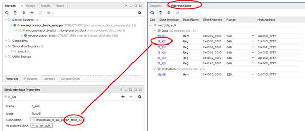
In this way you can see which address is assigned to each peripheral by checking the diagram:
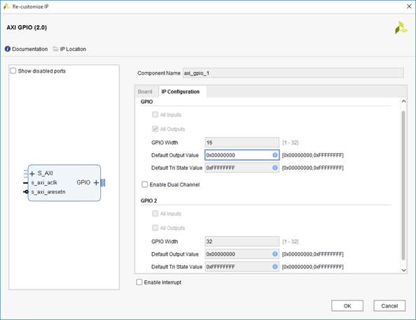
2. By double-clicking each block in the diagram, you can see the parameters of each block, for example the parameters of GPIO connected to leds_16bits are as follows:
Conclusion
Using Vivado, block diagram creation and automation wizards, you have created the microprocessor hardware. In a future lab in this course, you will learn how to create the software for this hardware platform, how to add other cores and debug the design.
Results required to complete the exercise
- Answer the questions in the test: https://docs.google.com/forms/d/e/1FAIpQLSewX0GSZ5gNjftalPaptU5nWcNseXTmrwzV-DX-Y0xe44vz9A/viewform?usp=sf_link
- There is no need to present this lab to the teacher, just go the the next lab.
Change history
Adaptation to version Vivado 2018.3: M. Wójcikowski (08/2020).