

Lab 5: HW/SW System Debug
This text is based on teaching materials from Xilinx (www.xilinx.com).
Contents
Step 1: Adding logic analyzer Chipscope to the microprocessor system
Results required to complete the exercise
Introduction
This lab guides you through the process of debugging the processor system. Vivado and Xilinx SDK together with ChipScope will be used to have visibility into both the Hardware and Software of the system.
Setup
For this lab, you will need a Xilinx Nexys A7 FPGA Board and a USB cable. Connect the USB cable to the PC and the Nexys A7 Board to connector PROG/UART. With this cable, the programming of the FPGA will be done, as well as serial communication between the board and PC.
Step 1: Adding logic analyzer Chipscope to the microprocessor system
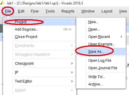
1. Open the project created in the lab4 and save it as a new project, for example lab5.
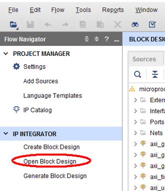
2. Click Open Block Design to edit the block diagram of the system:
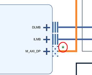
3. Right-click on the output bus M_AXI_DP of MicroBlaze and select Debug:
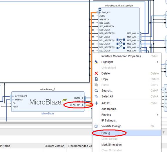
The symbol ![]() will appear next to the M_AXI_DP bus on the block diagram:
will appear next to the M_AXI_DP bus on the block diagram:
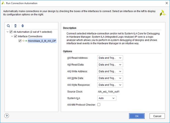
and the possibility to run Connection Automation wizard will appear in top left corner of the block diagram window. Run Connection Automation with default settings:
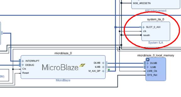
After running this wizard, you should notice a new block: Integrated Logic Analyzer (ILA) block with appropriate connections:
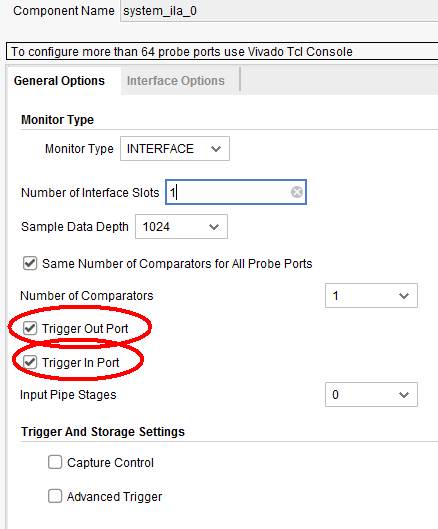
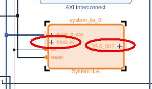
4. Now double-click on the newly added block system_ila, and select Trigger Out Port and Trigger In Port options, this will result in new ports in the ILA block:
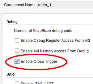
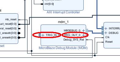
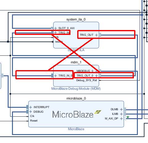
5. Double-click mdm block and select Enable Cross Trigger to add two ports TRIG_IN_0 and TRIG_OUT_0 to this block:
6. Run Connection Automation wizard and select all ports of MDM:
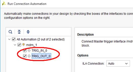
Now the blocks MDM and ILA will be cross-connected:
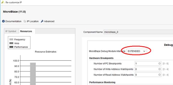
7. Finally, change the debug mode of the MicroBlaze: double-click on the MicroBlaze block and on page 3 of the setting window change MicroBlaze Debug Module Interface from BASIC to EXTENDED to enable cross-triggering:
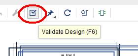
8. When you finish all the changes in block diagram, it is a good idea to perform validation:
9. Generate bitstream.
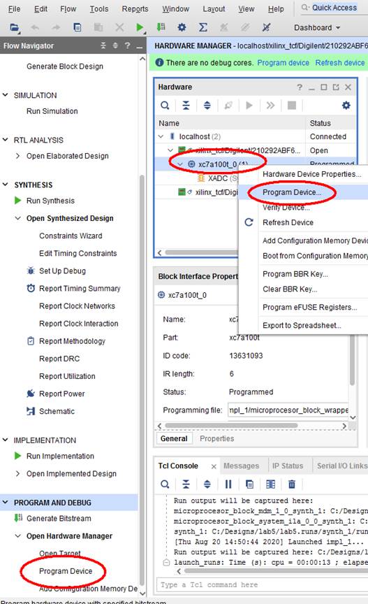
10. Program the FPGA from Vivado:
If you have problems with programming and you cannot manually reset the board (remote lab), check this document: Remote reset by JTAG.
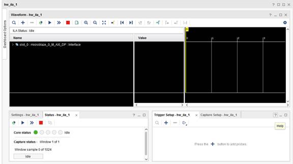
11. After successful programming, logic analyzer window will open, because your hardware now contains ILA block:
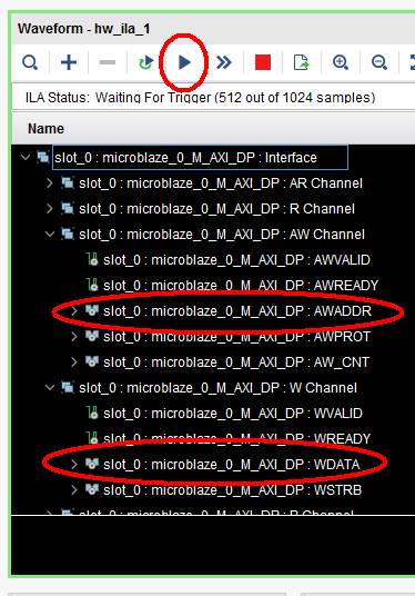
12. In trigger setup, add the probe to the write address bus microblaze_0_M_AXI_DP: AWADDR and write address valid signal microblaze_0_M_AXI_DP: AWVALID to detect write operation by the MicroBlaze to the selected address. Set the value of the trigger to the base address of your 7-segment display block. Set the value of “write valid” signal to ‘1’.
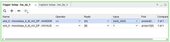
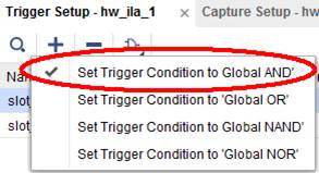
13. Check if logical condition for those signals is “AND”:
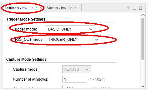
14. Change the trigger output in the Settings window, as shown below:
15. Click Run trigger ![]() and display the names of the observed signals as shown in the figure below. The signals which you will be observing are marked in red:
and display the names of the observed signals as shown in the figure below. The signals which you will be observing are marked in red:
If your software is not running, you should see “Waiting For Trigger” message.
16. Export hardware design to SDK, including the bitstream.
17. Launch Xilinx SDK.
18. Leave Vivado open, because you will use waveform window of the logic analyzer in next step.
Step 2: Running the debugger
If you have multiple hardware platform in your Xilinx SDK project, you should tell the BSP which platform to use. Right-click on BSP, select Properties and in Project reference section select the hardware platform you want to use (usually the newest one).
If you have more than one prototype board connected to your PC, you should follow the procedure given here: Working with multiple FPGAs connected to the PC.
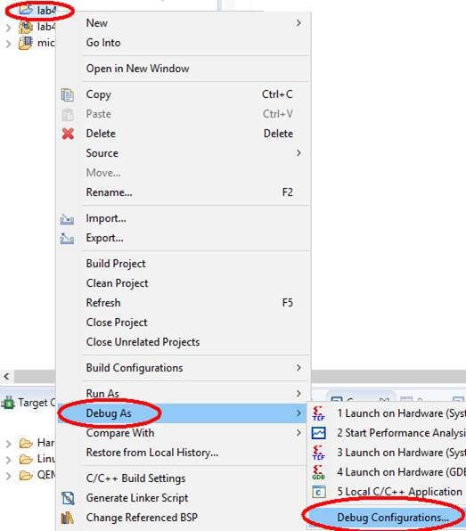
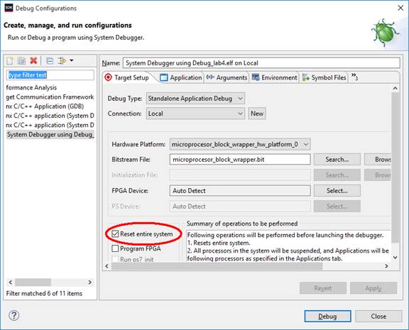
1. Set Reset entire system setting in Debug Configuration (the same as you did in the previous lab in Run Configuration):
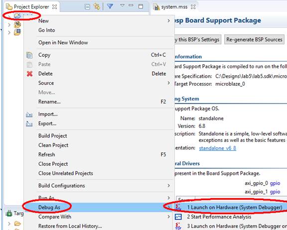
2. Run the same software as used in lab4 in debugger:
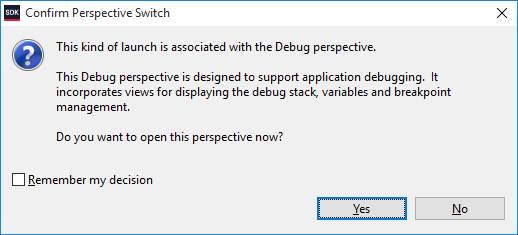
Xilinx SDK will ask, if you want to change the perspective:
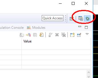
If you agree, you can always switch back to the normal perspective, using the buttons on the top-right corner of the screen:
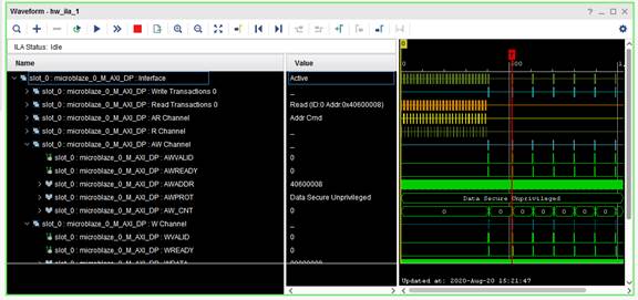
After running the software, you should see that the logic analyzer triggered and its waveform window contains the waveforms registered by ILA:
3. The logic analyzer’s status is now Idle. If you want to trigger new events, you need to click ![]() again.
again.
Conclusions
You have added the logic analyzer to your system, and configured it for cross-triggering. You run the software debugger together with the armed trigger of hardware logic analyzer. When the logic analyzer detects the triggered event, it also stops the debugger, so the user can see, at which line of the software the event happened.
Results required to complete the exercise
· Answer the questions in the test: https://docs.google.com/forms/d/e/1FAIpQLSfd8lYg12v1WXhhVd3nMrGUFq6NW6bcn_sK1a2CUthIJbnV1A/viewform?usp=sf_link
· Present to the teacher the cross-triggering of your system: you should run the software in debugger and simultaneously run logic analyzer. Set up the trigger to the write operation to LED display controller. When the logic analyzer detects the trigger condition, it should capture the signals to the waveform window and also it should stop the debugger at the command executed at the time of triggering the analyzer.
· Inspect what data is written to the 7-segment LED controller block during triggered write operation in the previous point. Explain this data.
Change history
Adaptation to version Vivado 2018.3: M. Wójcikowski (08/2020).